Multi-layer thick-film RF package

a technology of rf and package, applied in the field of rf power transistor packages, can solve the problems of higher manufacturing and labor costs, and inability to meet the requirements of a wide range of applications, so as to reduce migration and increase conductivity

Active Publication Date: 2011-10-11
MICROSEMI CORP
View PDF43 Cites 3 Cited by
  • Summary
  • Abstract
  • Description
  • Claims
  • Application Information

AI Technical Summary

Benefits of technology

[0011]In another example embodiment of the present invention, different materials are used for different parts of the RF package to increase conductivity and reduce migration between the conductive and dielectric layers. For example, some portions of the conductive layer can be formed using silver (Ag) thick-film paste, while other portions, specifically the bridge and drain portions, can be formed using gold (Au) thick-film paste. The dielectric layer includes openings in which electrical interfaces between the conductive portions and one or more dies can be formed using wire bonds. The dielectric layer also includes notches through which source leads, drain leads, and gate leads can be electrically coupled to source portions, drain portions, and gate portions, respectively, of the conductive layer(s).

Problems solved by technology

While the arrangement of such components can improve signal stability and integrity to some degree, producing such packages is costly.
Moreover, frequency stability and conductivity of the prior art parts is not necessarily optimal.
The mechanical construction and assembly of the separate components of the package result in higher manufacturing and labor costs, which is of critical importance when producing the packages in high quantities.
Moreover, lower electrical conductivity of the parts themselves inhibits the performance of the circuit components, leads, and other electrical parts associated with the package.

Method used


Image

  • Multi-layer thick-film RF package
  • Multi-layer thick-film RF package
  • Multi-layer thick-film RF package

Examples


Embodiment Construction

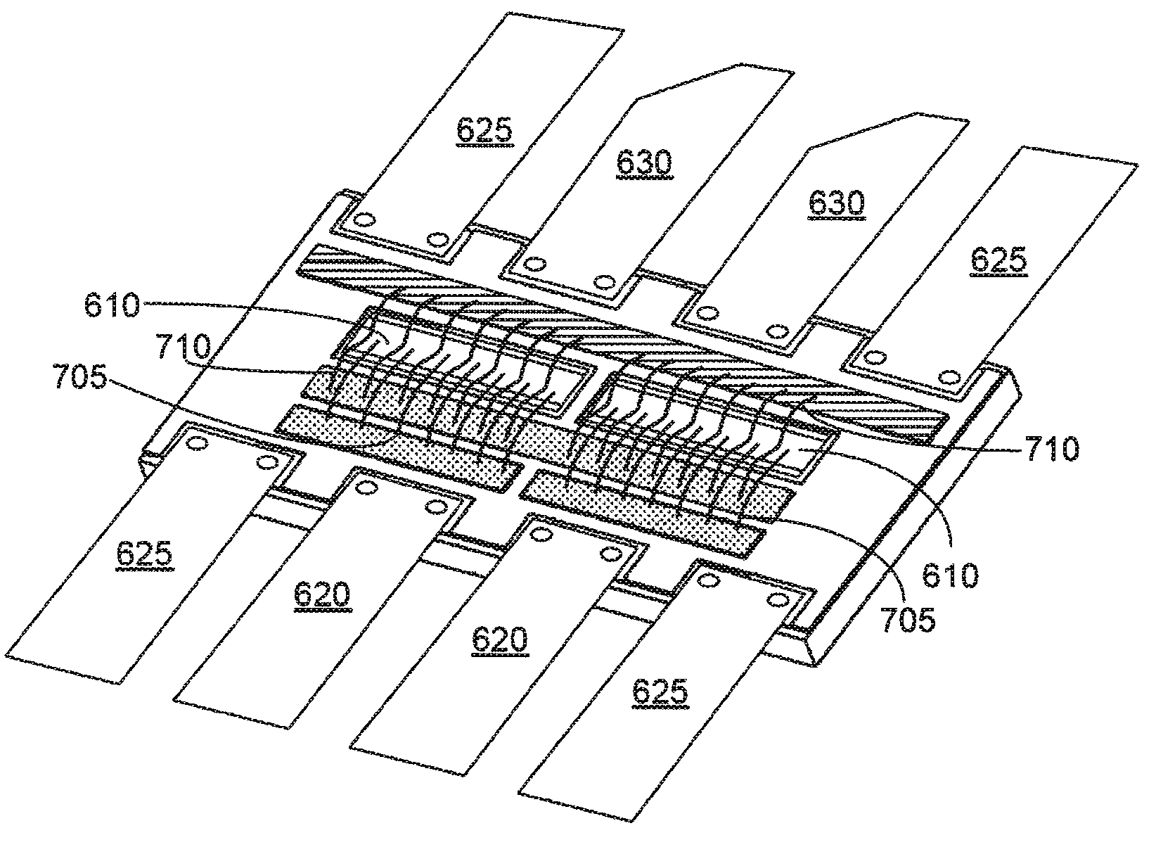
[0009]In an example embodiment of the invention, a multi-layer thick-film RF power transistor package is provided. The RF package is a single-piece, monolithic, sintered, high-frequency package having circuit features including a highly conductive and low capacitive source bridge.

[0010]A method of fabricating the RF package includes forming conductive layer(s) including one or more source portions, one or more gate portions, and / or one or more drain portions on a ceramic substrate. The conductive layer(s) and the ceramic substrate are fired or otherwise heated in a furnace until sintered. Thereafter, a dielectric pattern is formed on the conductive layer and fired or otherwise heated in the furnace until sintered. Then, a conductive bridge is formed on the dielectric pattern, over the one or more drain portions and between the one or more source portions, which is then fired until sintered in the furnace.

[0011]In another example embodiment of the present invention, different materia...


PUM

PropertyMeasurementUnit
conductiveaaaaaaaaaa
dielectricaaaaaaaaaa
stabilityaaaaaaaaaa

Abstract

A method for producing a multi-layer thick-film RF package includes forming conductive layer(s) including one or more source portions, one or more gate portions, and / or one or more drain portions on a ceramic substrate. The conductive layer(s) and the ceramic substrate are fired or otherwise heated in a furnace until sintered. Thereafter, a dielectric pattern is formed on the conductive layer(s) and fired or otherwise heated in the furnace until sintered. Then, a conductive bridge is formed on the dielectric pattern, over the one or more drain portions and between the one or more source portions, which is then fired until sintered in the furnace. As a result, a monolithic, single-piece, sintered, high-frequency RF power transistor package having circuit features including a highly conductive and low capacitive bridge is produced.

Description

CROSS REFERENCE TO RELATED APPLICATION[0001]This application claims the benefit of U.S. Provisional Patent Application Ser. No. 61 / 261,338, filed Nov. 15, 2009, herein incorporated by reference.BACKGROUND[0002]1. Technical Field[0003]This disclosure relates to RF power transistors, and more particularly to power transistor packages.[0004]2. Discussion of Related Art[0005]Conventional high frequency power transistor packages use of a variety of mechanical components to provide RF signal stability and integrity.[0006]For example, U.S. Pat. No. 3,555,375 entitled High Frequency Power Transistor Having Crossing Input and Output Leads describes a technique in which compensation for stray inductive feedback coupling is achieved by crossing input and output leads. Specifically, a high frequency transistor is described having input, output, and common leads. In order to reduce the unwanted feedback effect of a stray series inductance in the common lead, the output leads are arranged so as t...

Claims


Application Information

Patent Timeline
Patent Type & Authority Patents(United States)
IPC IPC(8): H01L21/50
CPCH01L23/15H01L24/48H01L24/49H01L25/072H01L2224/48091H01L2224/48227H01L2224/48472H01L2224/49175H01L2224/85439H01L2224/85444H01L2224/85464H01L2924/01014H01L2924/01046H01L2924/01047H01L2924/01079H01L2924/01082H01L2924/014H01L2924/13055H01L2924/13091H01L2924/15153H01L2924/15787H01L2924/30107H05K3/4667H01L2924/00014H01L2924/01033H01L2924/01075H01L2924/00H01L2224/49111H01L2924/10253H01L2224/45099
Inventor SAMPLES, BENJAMIN A.
Owner MICROSEMI CORP
Why Eureka
Try Eureka