Display device
a display device and display screen technology, applied in the field of display devices, can solve the problems of reducing the refractive index, reducing and the touch panel itself increasing the thickness and weight of the entire device or the cost, so as to achieve stable touch panel operation and suppress capacitive coupling
- Summary
- Abstract
- Description
- Claims
- Application Information
AI Technical Summary
Benefits of technology
Problems solved by technology
Method used
Image
Examples
first embodiment
of the Invention
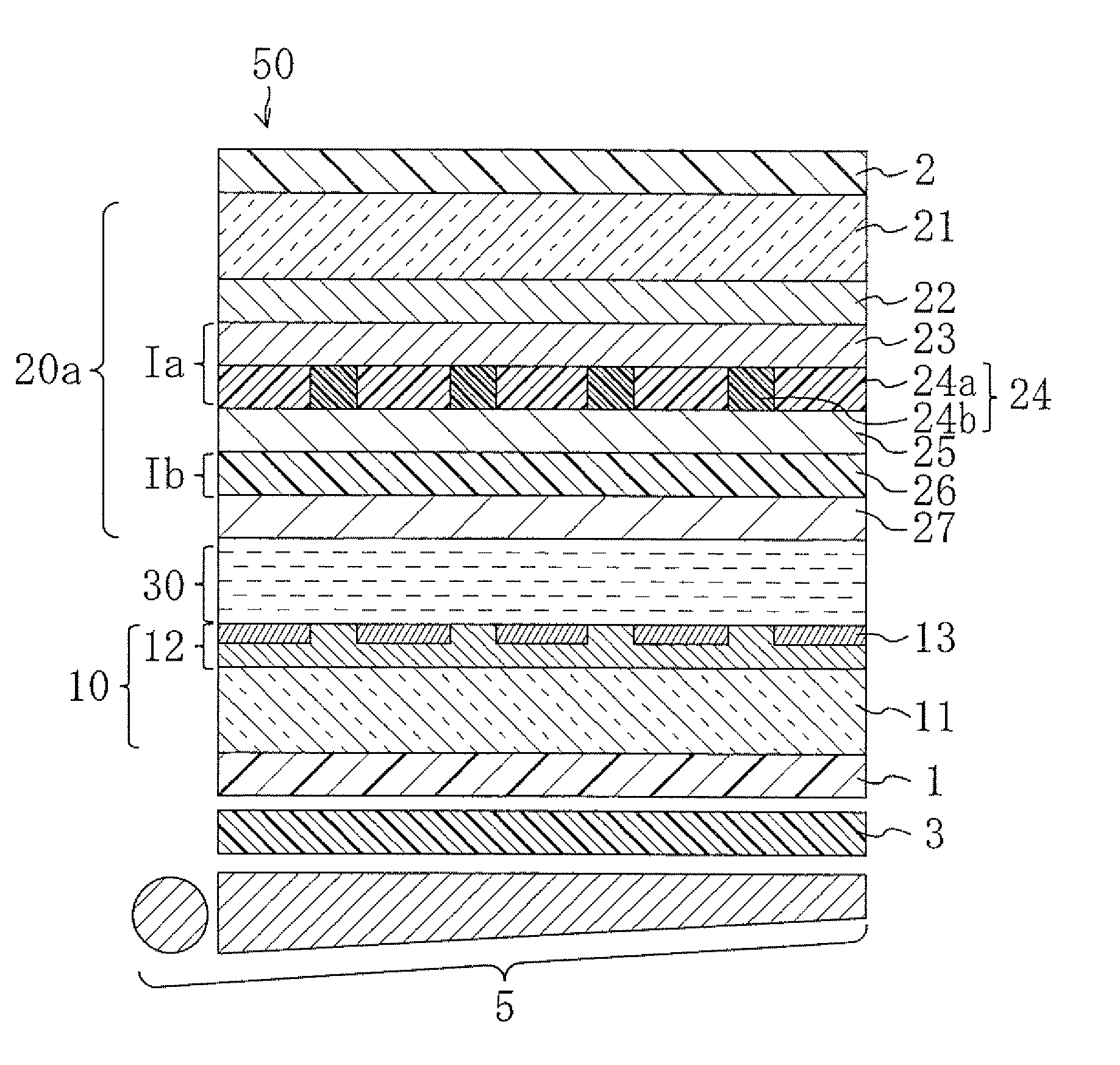
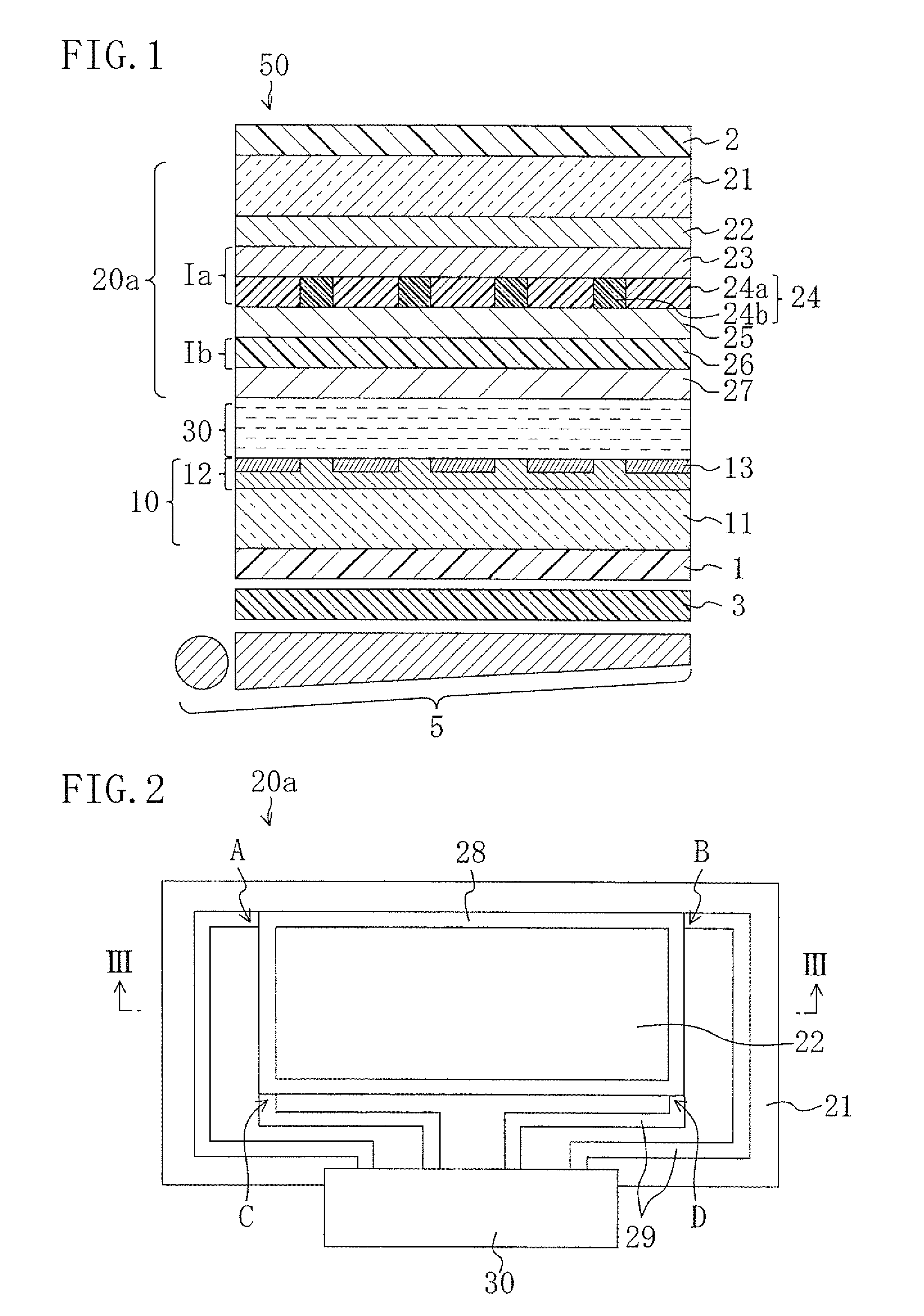
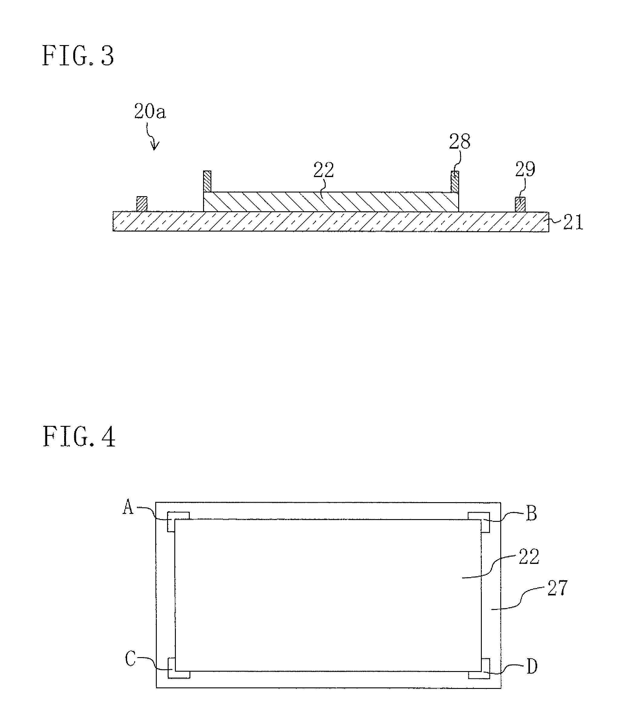
[0097]FIGS. 1 to 6 show a liquid crystal display device according to a first embodiment of the invention. Specifically, FIG. 1 is a schematic cross-sectional view of a liquid crystal display device 50 according to this embodiment. FIG. 2 is a schematic plan view of part of a touch panel 20a included in the liquid crystal display device 50, and FIG. 3 is a schematic cross-sectional view taken along the line III-III in FIG. 2.
[0098]As shown in FIG. 1, the liquid crystal display device 50 includes: an active matrix substrate 10; a touch panel substrate 20a disposed to face the active matrix substrate 10; a liquid crystal layer 30 as a display medium layer interposed between the active matrix substrate 10 and the touch panel substrate 20a; a back light 5 placed under the active matrix substrate 10 with a polarizing plate 1 and a diffusion sheet 3 interposed therebetween; and a polarizing plate 2 formed on the touch panel substrate 20a.
[0099]The active matrix substrate 1...
second embodiment
of the Invention
[0167]FIG. 7 is a schematic cross-sectional view of a touch panel substrate 20b included in a liquid crystal display device according to this embodiment. In the following embodiments, the same members as those shown in FIGS. 1 to 6 are identified by the same reference numerals and detailed description thereof will be omitted herein.
[0168]The liquid crystal display device of this embodiment includes the touch panel substrate 20b in place of the touch panel substrate 20a of the first embodiment.
[0169]In the touch panel substrate 20b, the positional relationship between a color filter layer 24 and a shield electrode 25 is opposite to that in the touch panel substrate 20a of the first embodiment. In the other respects, the configuration of the touch panel substrate 20b is the same as that of the touch panel substrate 20a.
[0170]The touch panel substrate 20b is prepared just by interchanging the process step of forming the color filter layer 24 and the process step of for...
third embodiment
of the Invention
[0173]FIG. 8 is a schematic cross-sectional view of a touch panel substrate 20c included in a liquid crystal display device according to this embodiment.
[0174]The liquid crystal display device of this embodiment includes the touch panel substrate 20c in place of the touch panel substrate 20a of the first embodiment.
[0175]In the touch panel substrate 20c, which is obtained by forming an organic insulating layer 26a between the color filter layer 24 and the shield electrode 25 in the touch panel substrate 20a of the first embodiment, a shield electrode 25 is sandwiched between a pair of organic insulating layers 26a and 26b. In the other respects, the configuration of the touch panel substrate 20c is the same as that of the touch panel substrate 20a.
[0176]In the liquid crystal display device including the touch panel substrate 20c of this embodiment, since the shield electrode 25 is formed between a first transparent electrode 22 and a second transparent electrode 27 ...
PUM
| Property | Measurement | Unit |
|---|---|---|
| thickness | aaaaa | aaaaa |
| thickness | aaaaa | aaaaa |
| thickness | aaaaa | aaaaa |
Abstract
Description
Claims
Application Information
 - R&D
- Intellectual Property
- Life Sciences
- Materials
- Tech Scout
- Unparalleled Data Quality
- Higher Quality Content
- 60% Fewer Hallucinations
Browse by: Latest US Patents, China's latest patents, Technical Efficacy Thesaurus, Application Domain, Technology Topic, Popular Technical Reports.
© 2025 PatSnap. All rights reserved.Legal|Privacy policy|Modern Slavery Act Transparency Statement|Sitemap|About US| Contact US: help@patsnap.com


