
Semiconductor device and method for cutting electric fuse

a technology of electric fuse and semiconductor, which is applied in the direction of semiconductor/solid-state device details, radio frequency controlled devices, instruments, etc., can solve the problems of defective cutting, electric fuse acquisition a lukewarm electric resistance, and incomplete cutting of fuse links

Inactive Publication Date: 2011-08-02
RENESAS ELECTRONICS CORP
View PDF8 Cites 8 Cited by
  • Summary
  • Abstract
  • Description
  • Claims
  • Application Information

AI Technical Summary

Benefits of technology

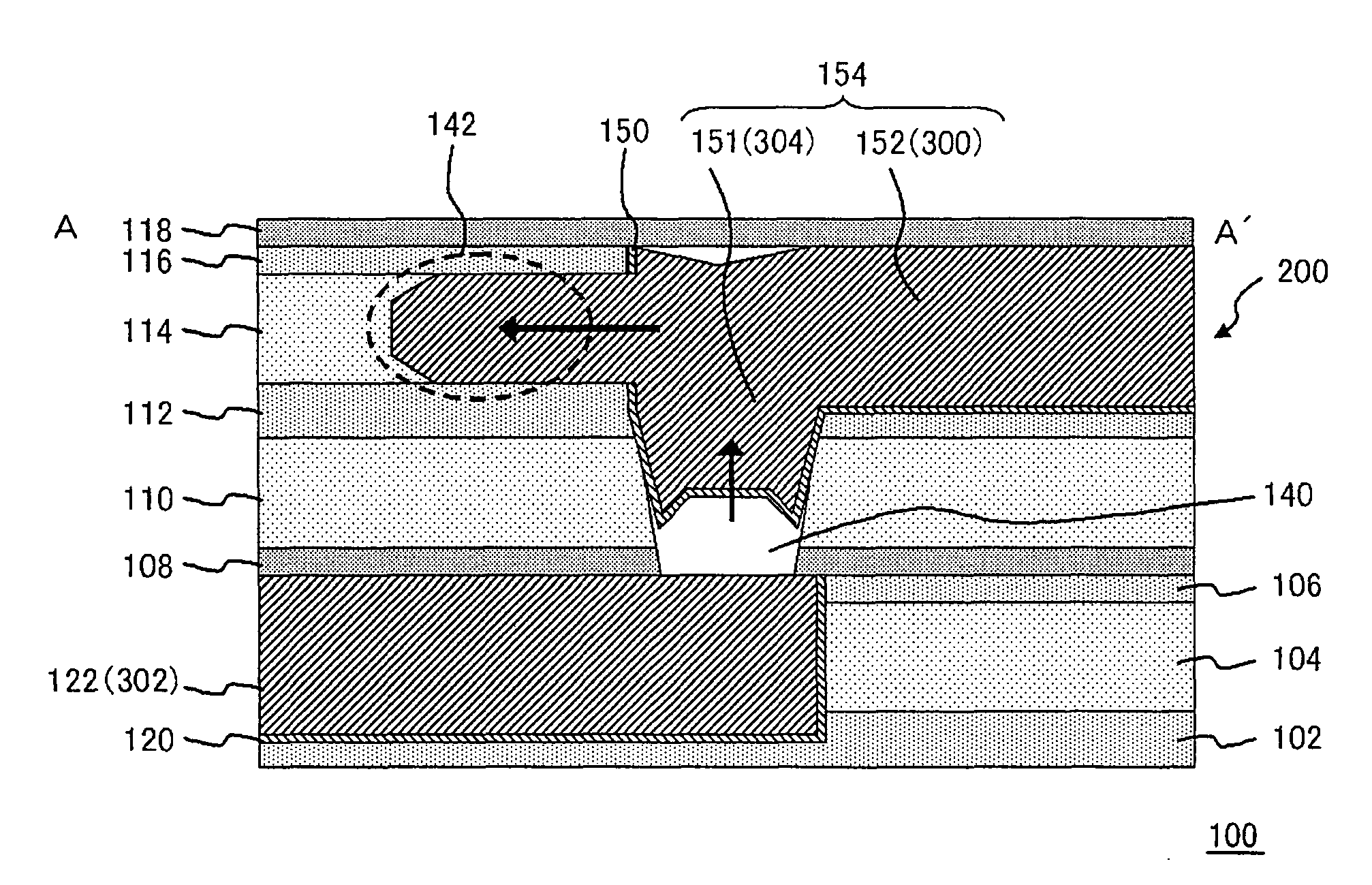
The present invention provides a method for cutting an electric fuse in a semiconductor device by applying a predetermined electric voltage across both ends of the first interconnect to allow an electric conductor that constitutes the first interconnect flowing from the first interconnect toward outside thereof, and thereby an electric conductor that constitutes the fuse link is migrated toward the first interconnect to form a void region in the fuse link. This method allows for a retrial of the operation for cutting the electric fuse and ensures an improved condition in cutting or breaking of the fuse link. The invention also provides a semiconductor device including the electric fuse and a method for manufacturing the semiconductor device.

Problems solved by technology

Nevertheless, when an electric current is applied to a fuse link to break thereof, an incomplete cutting of the fuse link is often caused to occur a defective cutting.
If such defective cutting of a fuse link is occurred, the electric fuse acquires a lukewarm electric resistance.
Therefore, a problem is caused, in which a decision circuit decided that the fuse is not cut, in case that it must be decided that the fuse is cut.
On the other hand, since the electric fuse acquires an increased electric resistance, a level of an electric current that requires for cutting the fuse can not be flowed when an electric current is flowed once again to break the fuse link.

Method used


Image

  • Semiconductor device and method for cutting electric fuse
  • Semiconductor device and method for cutting electric fuse
  • Semiconductor device and method for cutting electric fuse

Examples


Embodiment Construction

[0035]The invention will be now described herein with reference to illustrative embodiments. Those skilled in the art will recognize that many alternative embodiments can be accomplished using the teachings of the present invention and that the invention is not limited to the embodiments illustrated for explanatory purposed.

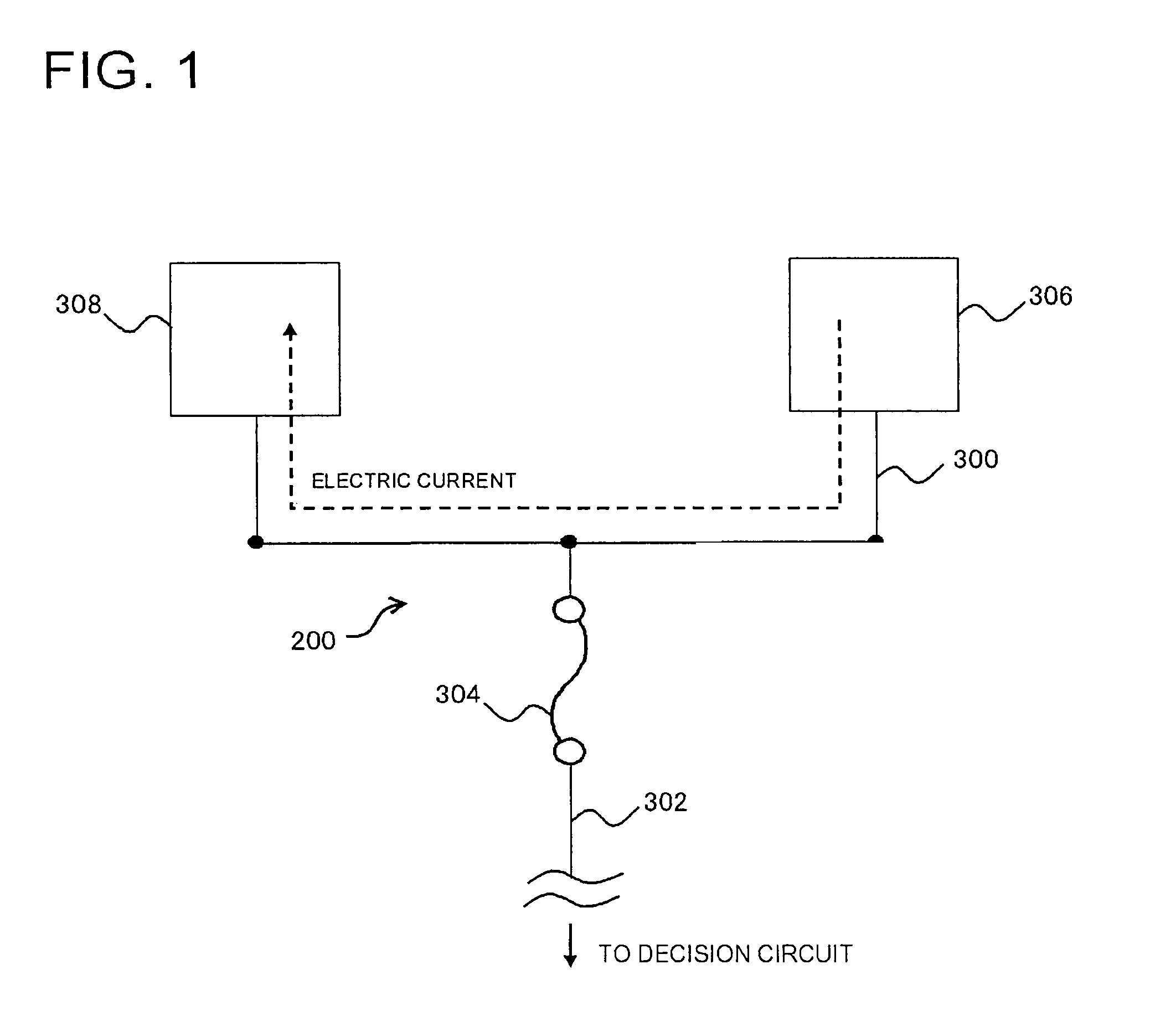
[0036]FIG. 1 is a layout diagram, showing a configuration of an electric fuse 200 in the present embodiment. The electric fuse 200 is composed of a fuse link 304, a first interconnect 300 coupled to one end of the fuse link 304, and an electric current inflow terminal 306 and an electric current drain terminal 308 formed in one end and another end of the first interconnect 300, respectively. The fuse link 304 is provided between the first interconnect 300 and the second interconnect 302, and functions as creating an electrical coupling or cutting between the first interconnect 300 and the second interconnect 302. In a condition before cutting the fuse link, anoth...


PUM


Abstract

An electric fuse includes: a first interconnect and a second interconnect, formed on a semiconductor substrate; a fuse link, formed on the semiconductor substrate and provided so that an end thereof is coupled to the first interconnect, the fuse link being capable of electrically cutting the second interconnect from the first interconnect; and an electric current inflow terminal and an electric current drain terminal for cutting the fuse link, formed on the semiconductor substrate and provided in one end and another end of the first interconnect, respectively.

Description

[0001]This application is based on Japanese patent application No. 2006-135,622, the content of which is incorporated hereinto by reference.BACKGROUND[0002]1. Technical Field[0003]The present invention relates to a semiconductor device and a method for cutting electric fuse, and particularly relates to a semiconductor device including an electric fuse and a method for cutting such electric fuse.[0004]2. Related Art[0005]A technology is conventionally known, in which a fuse is mounted in a semiconductor device, and the fuse is cut, so that a value of a resistor employed in the semiconductor device is suitably adjusted, or a failure element is separated and replaced into a normal element.[0006]Typical manner for cutting a fuse includes cutting a fuse by irradiating a laser beam in a portion of the fuse and cutting a fuse by applying an electric current.[0007]U.S. Pat. No. 4,064,493, Japanese Laid-open patent publication No. 2005-39,220 and Japanese Laid-open patent publication No. 200...

Claims


Application Information

Patent Timeline
Patent Type & Authority Patents(United States)
IPC IPC(8): H01L29/68H01L27/148
CPCG11C17/16G11C17/18H01L23/5256H01L2924/0002H01L2924/00
Inventor UEDA, TAKEHIRO
Owner RENESAS ELECTRONICS CORP
Learn More