Methods for growing low-resistivity tungsten for high aspect ratio and small features
a technology of low-resistance tungsten and nucleation layers, which is applied in the direction of coatings, chemical vapor deposition coatings, metallic material coating processes, etc., can solve the problems of limited ability to provide nucleation layers for the deposition of low-resistance tungsten in small features with high aspect ratios, and cannot be produced easily and reliably. , to achieve the effect of low-resistan
- Summary
- Abstract
- Description
- Claims
- Application Information
AI Technical Summary
Benefits of technology
Problems solved by technology
Method used
Image
Examples
example 1
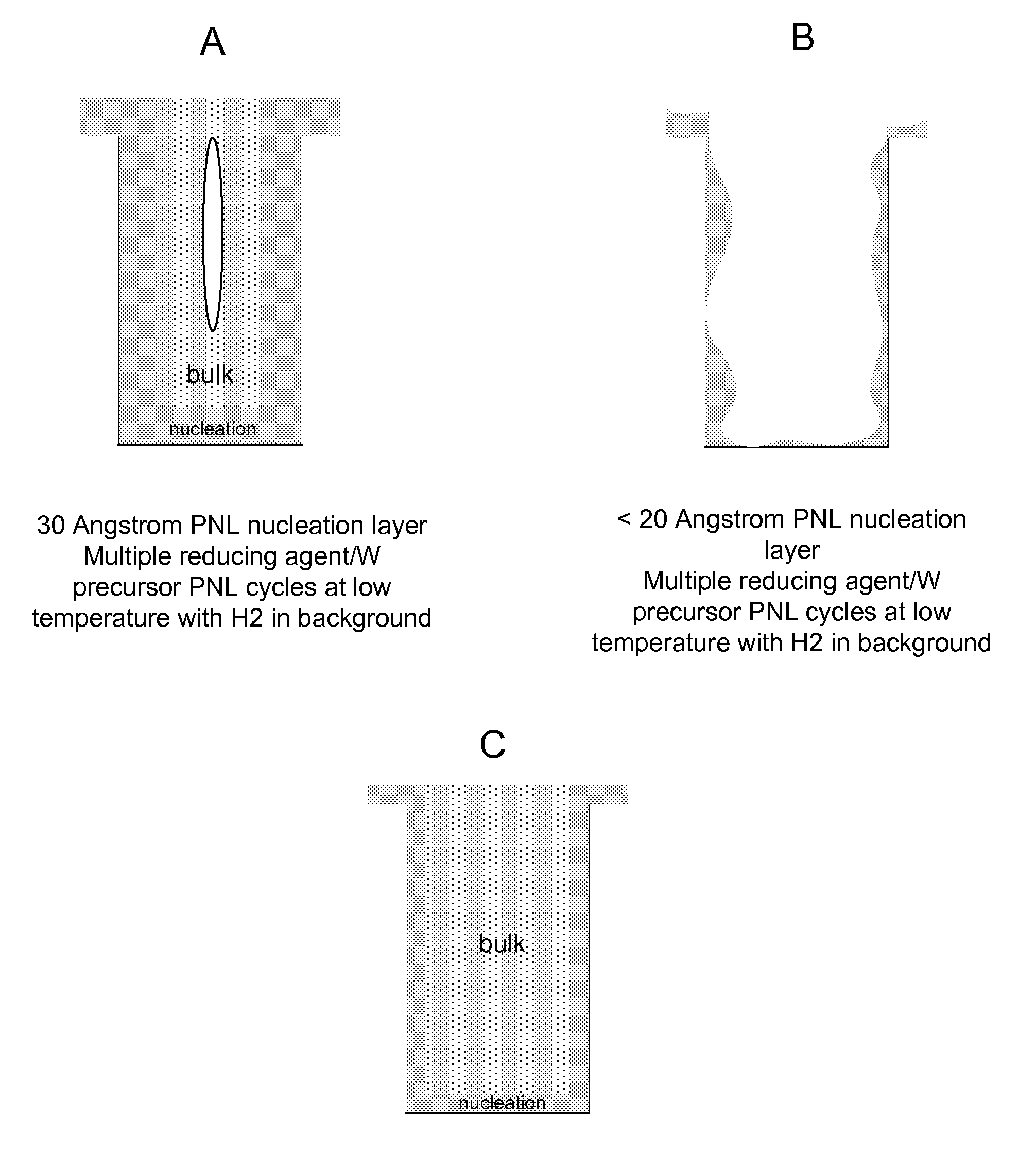
[0037]A W nucleation layer was formed in a feature having an AR of 30:1 and a 0.15 μm opening the following pulsed nucleation layer process:
5 Torr, 300 C, B2H6 dose (7.5 sec.), 10 sec. purge, WF6 dose (10 sec)
A W bulk layer was then formed using a CVD process (H2-WF6) at 80 Torr and 395 C.
[0038]The thickness of the nucleation layer was about 80 Angstroms. Total thickness was 2000 Angstroms. Resistivity was of the film as measured on a blanket wafer was 11 μΩ-cm. Step coverage was greater than 90%.
example 2
[0039]A W nucleation layer was formed in a feature having a 10:1 AR and a 0.075 μm opening using the following pulsed nucleation layer process:
40 Torr, 300 C, B2H6 dose (1 sec.), 3 sec. purge, WF6 dose (0.5 sec), 3 sec purge (5 cycles)
W bulk layer was then formed using a CVD process (H2-WF6) at 40 Torr and 395 C.
[0040]The thickness of the nucleation layer was about 20 Angstroms. Total thickness was 2000 Angstroms. Resistivity was of the film as measured on a blanket wafer was 11 μΩ-cm. Step coverage was greater than 90%.
[0041]Apparatus
[0042]The methods of the invention may be carried out in various types of deposition apparatus available from various vendors. Examples of suitable apparatus include a Novellus Concept-1 Altus, a Concept 2 Altus, a Concept-2 ALTUS-S, a Concept 3 Altus deposition system, or any of a variety of other commercially available CVD tools. In some cases, the process can be performed on multiple deposition stations sequentially. See, e.g., U.S. Pat. No. 6,143,0...
PUM
| Property | Measurement | Unit |
|---|---|---|
| width | aaaaa | aaaaa |
| temperature | aaaaa | aaaaa |
| temperature | aaaaa | aaaaa |
Abstract
Description
Claims
Application Information
 - R&D
- Intellectual Property
- Life Sciences
- Materials
- Tech Scout
- Unparalleled Data Quality
- Higher Quality Content
- 60% Fewer Hallucinations
Browse by: Latest US Patents, China's latest patents, Technical Efficacy Thesaurus, Application Domain, Technology Topic, Popular Technical Reports.
© 2025 PatSnap. All rights reserved.Legal|Privacy policy|Modern Slavery Act Transparency Statement|Sitemap|About US| Contact US: help@patsnap.com


