Balance-unbalance conversion element
a technology of unbalance and conversion element, applied in the direction of waveguides, waveguide devices, electrical devices, etc., can solve the problem of narrow frequency band where proper balance characteristics can be obtained, and achieve the effect of restricting the electrode pattern
- Summary
- Abstract
- Description
- Claims
- Application Information
AI Technical Summary
Benefits of technology
Problems solved by technology
Method used
Image
Examples
Embodiment Construction
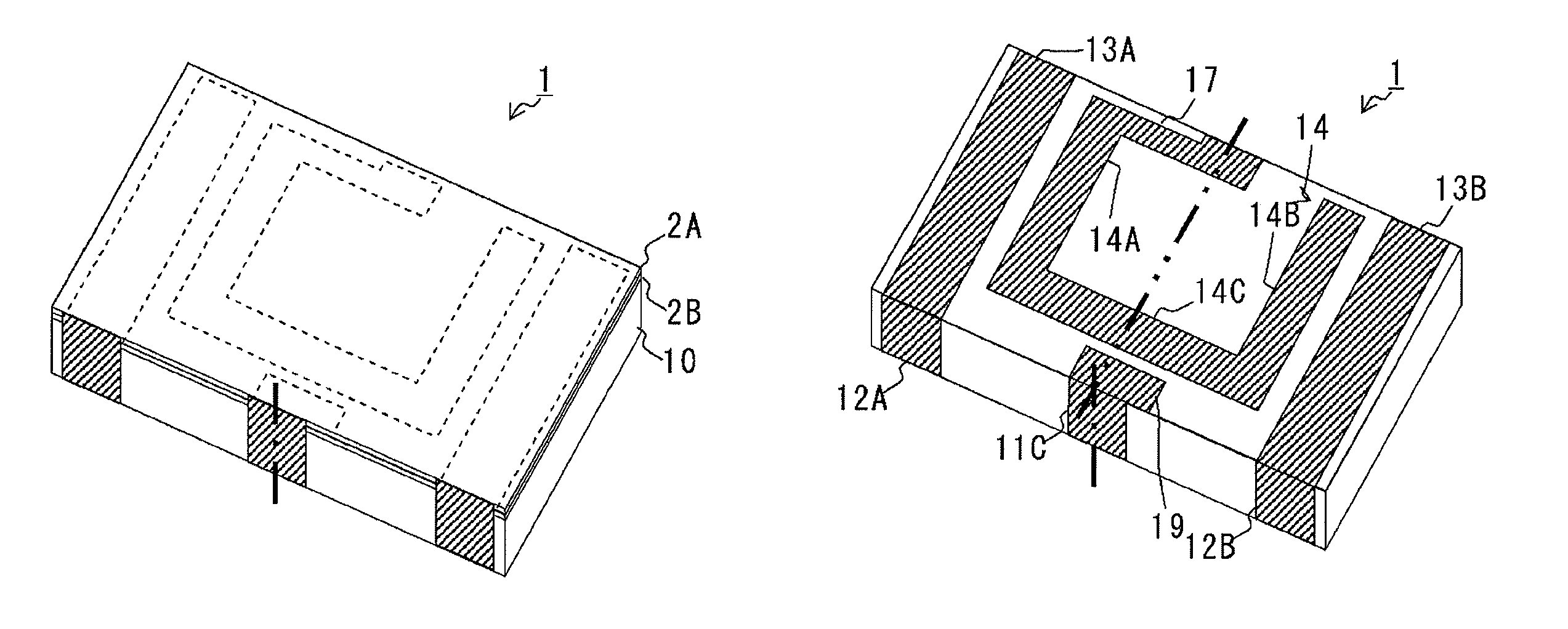
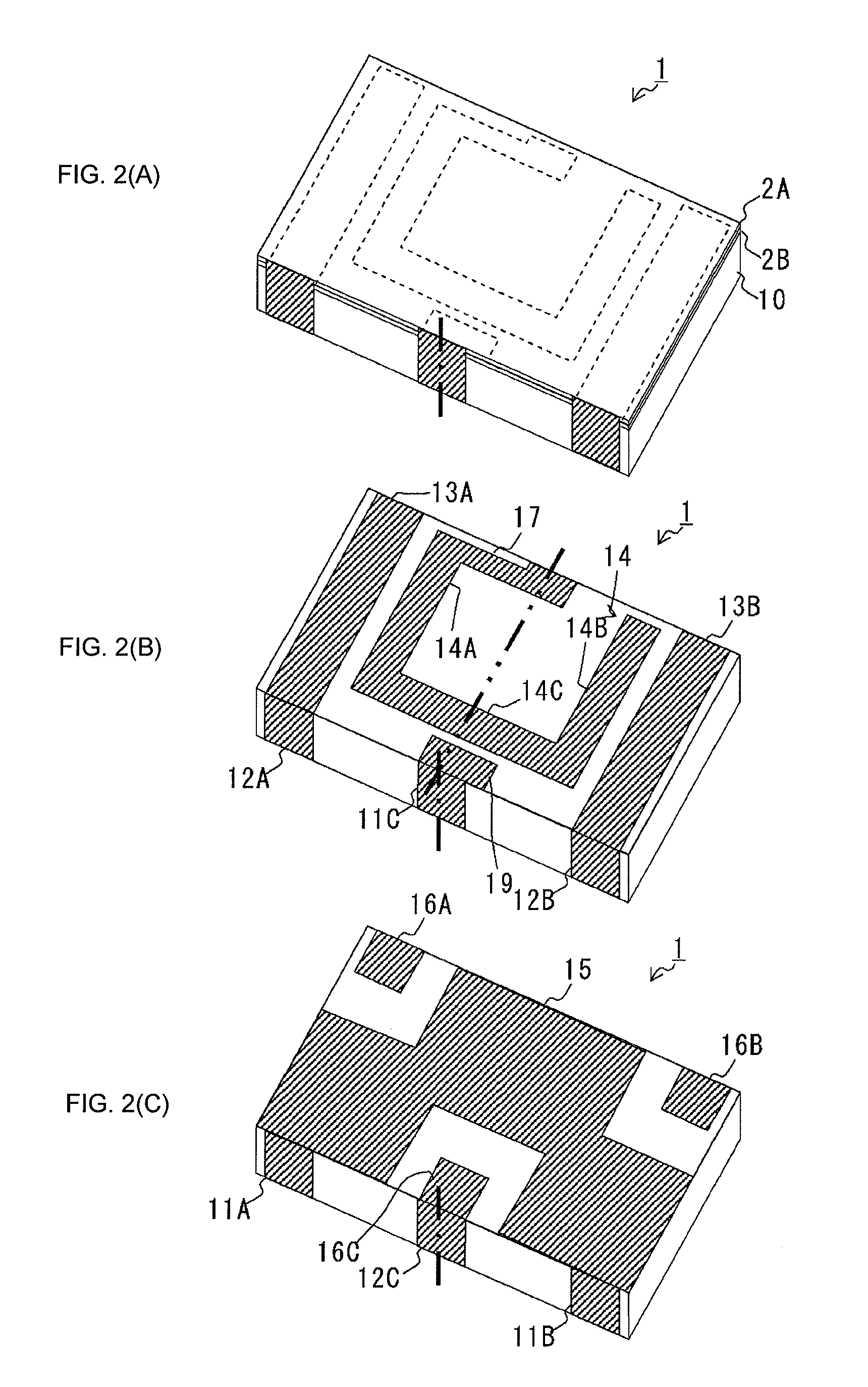
[0035]FIGS. 2(A) to 2(C) are drawings showing a configuration of a balance-unbalance conversion element. FIG. 2A is a perspective view of the top surface of the balance-unbalance conversion element. The left front side of the drawing is the front surface of the balance-unbalance conversion element and the right front side of the drawing is the right side surface thereof.
[0036]A balance-unbalance conversion element 1 is a balun element taking the shape of a small rectangular parallelepiped and to be used in UWB (ultra wide band) communications. The balance-unbalance conversion element 1 has a configuration where the top surface of a rectangular plate-shaped dielectric substrate 10 is covered with glass layers 2A and 2B. The glass layer 2B is a translucent glass layer and the glass layer 2A is a lightproof glass layer.
[0037]As for the external dimensions of the balance-unbalance conversion element 1 where the substrate thickness of the dielectric substrate 10 is 500 μm and the thickne...
PUM
 Abstract
Description
Claims
Application Information
 - R&D
- Intellectual Property
- Life Sciences
- Materials
- Tech Scout
- Unparalleled Data Quality
- Higher Quality Content
- 60% Fewer Hallucinations
Browse by: Latest US Patents, China's latest patents, Technical Efficacy Thesaurus, Application Domain, Technology Topic, Popular Technical Reports.
© 2025 PatSnap. All rights reserved.Legal|Privacy policy|Modern Slavery Act Transparency Statement|Sitemap|About US| Contact US: help@patsnap.com


