Passive spectrum control for pulsed RF power amplifiers
a power amplifier and pulsed rf technology, applied in the field of electronic devices, can solve the problems of poor performance at extreme temperatures, large footprint, and low cost, and achieve the effects of poor performance, large footprint, and high cos
- Summary
- Abstract
- Description
- Claims
- Application Information
AI Technical Summary
Benefits of technology
Problems solved by technology
Method used
Image

Examples
example 1
[0034]An RF power amplifier including an example of a microstrip filter / matching network combination was simulated as follows. In this example, the filter / matching network combination was placed between the first and second stages of the RF amplifier. The first stage included an APT 7 Watt (W) RF transistor 410 having an output impedance of 6.5-j10 Ohms. The second stage included an Integra 140 W transistor having an input impedance of 6.8+j7.2 Ohms.
[0035]FIG. 5 illustrates the RF CAD (computer aided design) design for this example microstrip filter / matching network. The terminations 505 and 510 were specified with the above-mentioned output and input impedances of the first and second stage RF transistors, respectively. Capacitors 515 and 520 are shunt capacitors to ground. In one simulation, capacitor 515 had a value of 3.73 picofarads (pF) and capacitor 520 had a value of 4.005 pF. In one simulation, capacitor 525 was given a value of 50 pF. Capacitors 515, 520 and 525 represent ...
example 2
[0046]An RF power amplifier including an example of a hybrid microstrip and discrete LC filter / matching network combination was simulated as follows. In this example, the filter / matching network combination was placed between the second and third stages of the RF amplifier. The second stage included a high power class C amplifier RF transistor having an output impedance of 4.3-j0.5 Ohms. The third stage also included a high power class C amplifier RF transistor having an input impedance of 1.77+j1.63 Ohms.
[0047]FIG. 7 illustrates the RF CAD design for this example hybrid filter / matching network. The terminations 605 and 610 were specified with the above-mentioned output and input impedances of the second and third stage RF transistors, respectively. As discussed above, the hybrid example includes both discrete capacitors 615, 620 and inductors 625, 630, as well as microstrip lines 635-660. In one simulation, capacitor 615 was given a value of 3.65 pF and capacitor 620 was given a va...
example 3
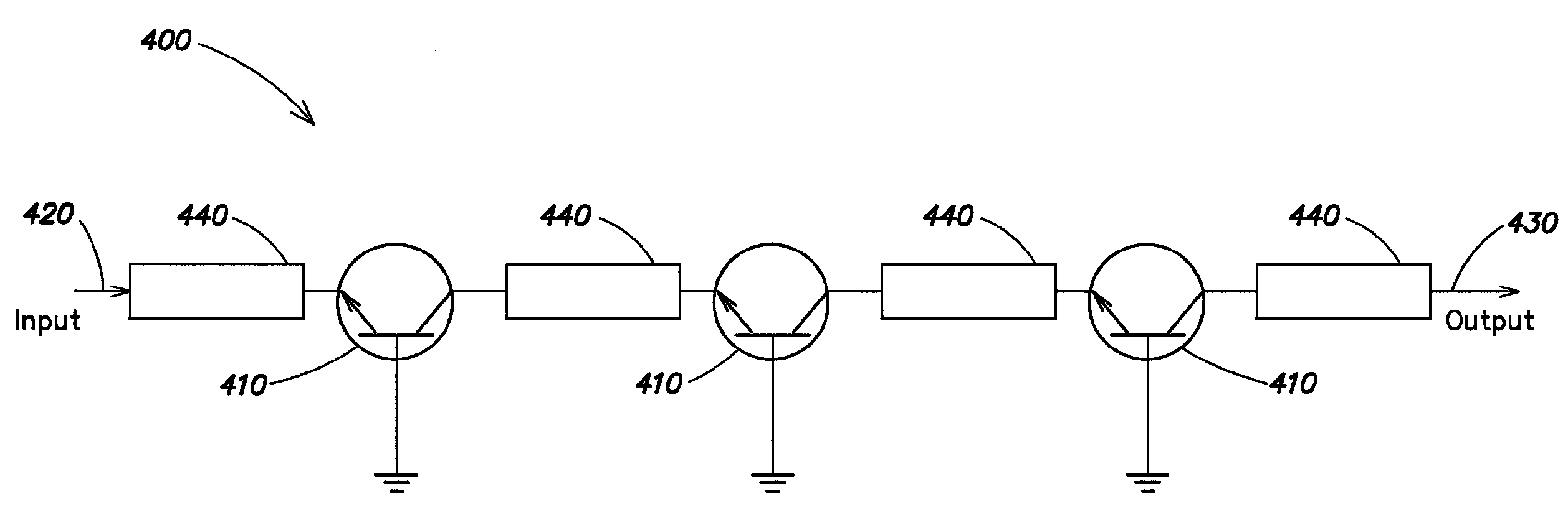
[0058]An example three stage RF power amplifier with a microstrip impedance matching / microstrip step bandpass filter combination was fabricated. This example RF power amplifier used an input RF power of 1 Watt and provided an output power of 800 Watts. The footprint of this RF power amplifier was 4.5 inches by 2.5 inches. These dimensions are comparable to those of a similar three-stage RF power amplifier using one of the conventional frequency spectrum control methods discussed above.
PUM
 Abstract
Description
Claims
Application Information
 - R&D
- Intellectual Property
- Life Sciences
- Materials
- Tech Scout
- Unparalleled Data Quality
- Higher Quality Content
- 60% Fewer Hallucinations
Browse by: Latest US Patents, China's latest patents, Technical Efficacy Thesaurus, Application Domain, Technology Topic, Popular Technical Reports.
© 2025 PatSnap. All rights reserved.Legal|Privacy policy|Modern Slavery Act Transparency Statement|Sitemap|About US| Contact US: help@patsnap.com