
Contamination pinning for auger analysis

Inactive Publication Date: 2010-12-21
KLA TENCOR CORP
View PDF12 Cites 6 Cited by
  • Summary
  • Abstract
  • Description
  • Claims
  • Application Information

AI Technical Summary

Benefits of technology

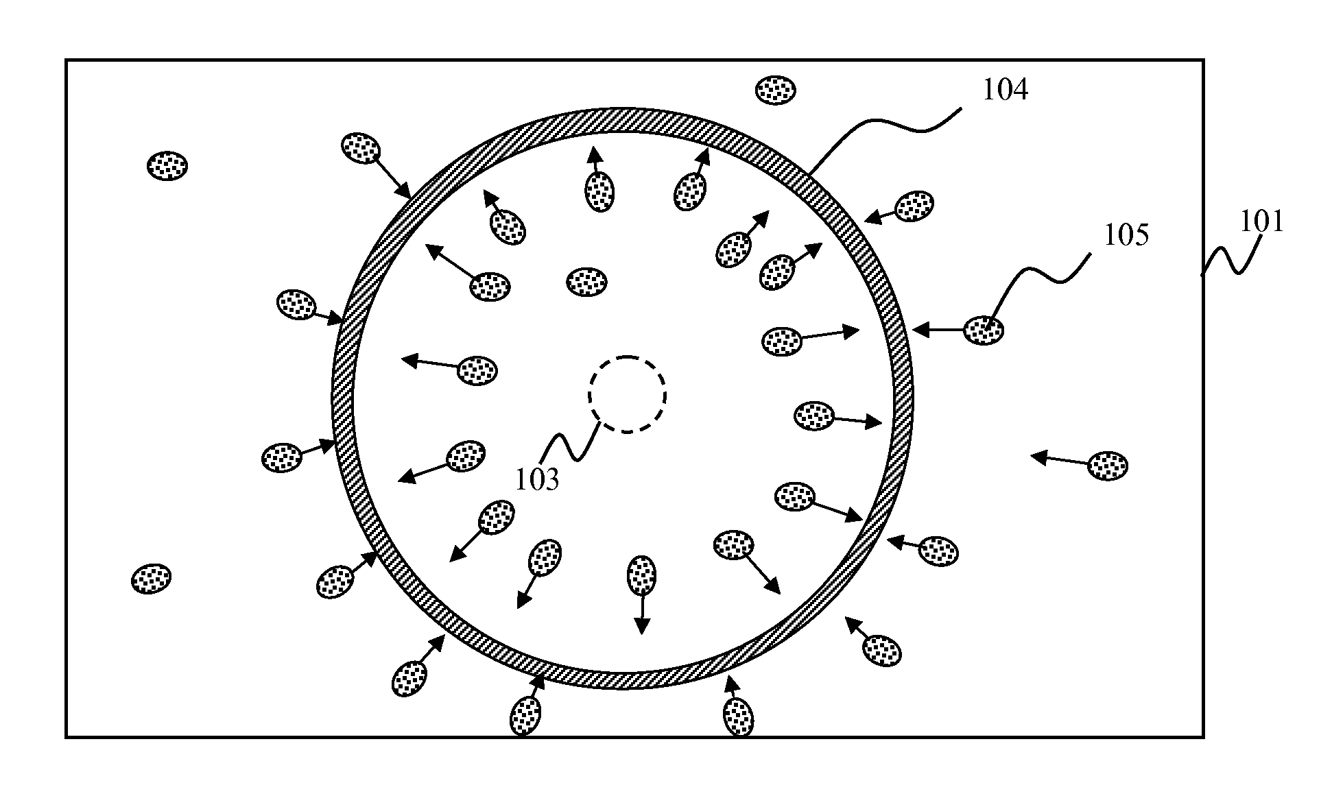
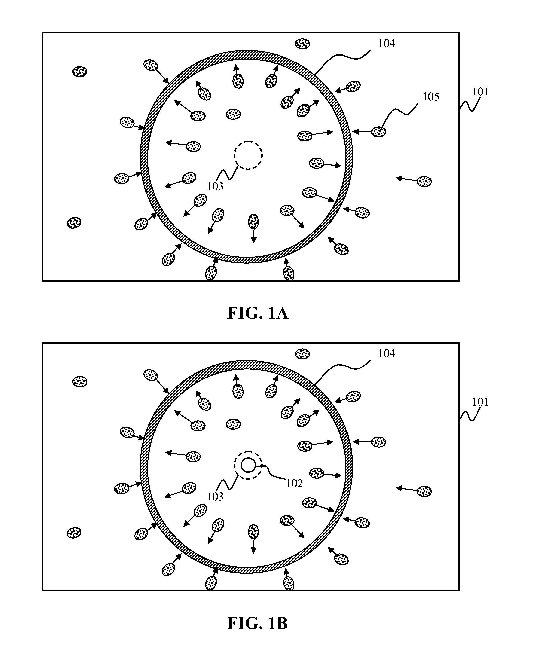
[0016]Embodiments of the present invention take advantage of the fact that contaminants tend to migrate towards places where electrons bombard a surface. Specifically, to keep contaminants away from a measurement location that is bombarded by primary electrons, the contaminants may be pinned by a pinning flux of electrons directed to one or more pinning regions on the surface. If the pinning regions are properly located, sized and shaped and the flux of electrons to the pinning regions is sufficiently large contaminants may be preferably attracted to or “pinned” to the pinning regions. This approach is somewhat counterintuitive in that it solves the contamination problem by taking advantage of the very phenomenon (attraction of the contaminants to target regions subject to electron bombardment) that leads to the contamination problem.
[0019]In embodiments of the present invention, the pinning flux may delay a buildup of adsorbates (including contaminants such as hydrocarbons) that would otherwise interfere with an Auger electron spectroscopy measurement. Thus, by pinning the contaminants, an Auger spectrum may be obtained at a higher chamber pressure than would otherwise be possible with a conventional Auger system.
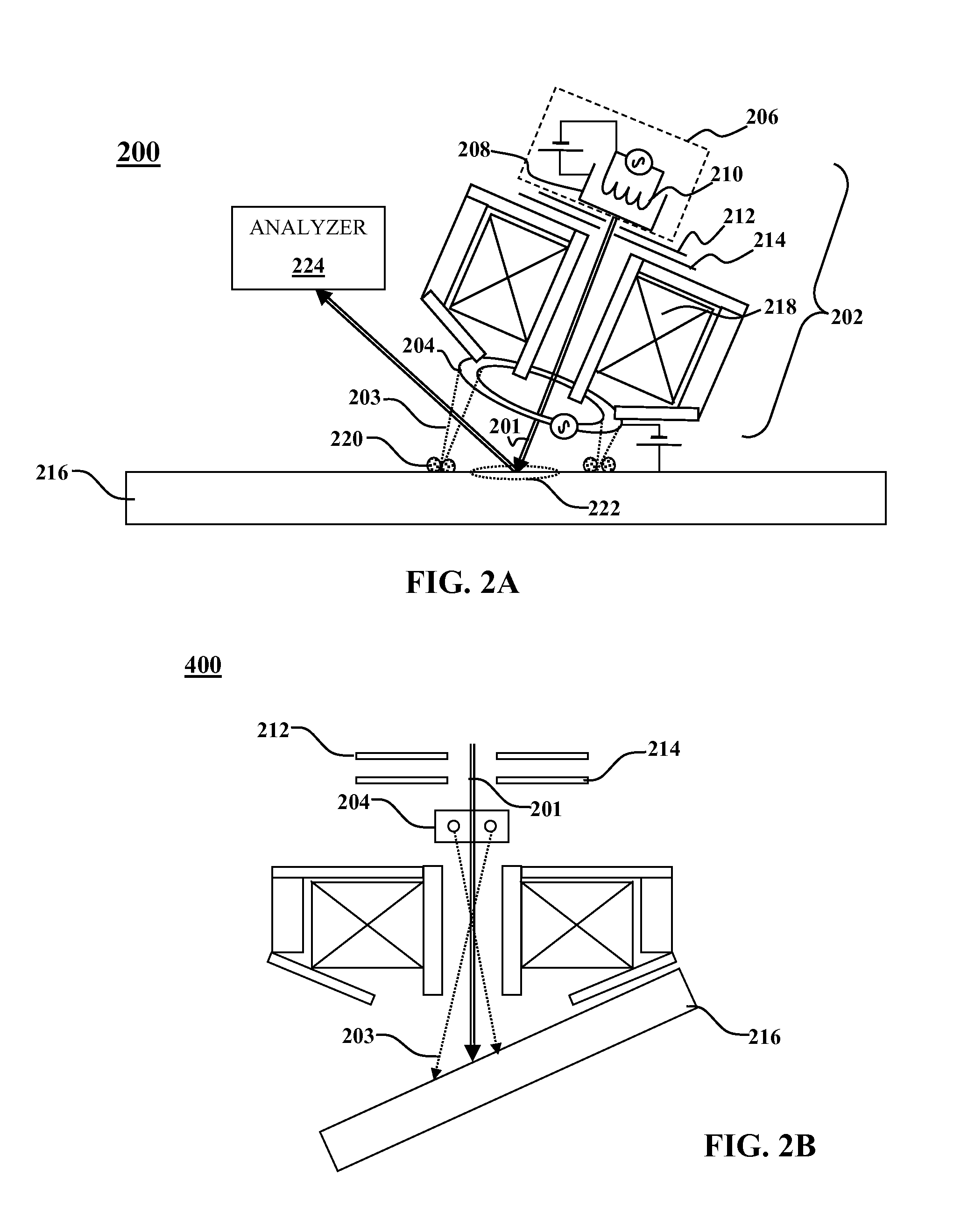
[0033]In some embodiments, a single beam steering mechanism 310 in the optical column 302 may have dual use where they are driven by a fast signal for drawing the pinning box 314 superimposed on a static signal that steers a primary beam spot in the region of interest 316. This allows an existing electron beam column to be used in embodiments of the present invention without having to add or modify any of its components. In alternative embodiments it may be better to use an additional separate dedicated beam steering mechanism 311 coupled to the controller 312 to draw the pinning box 314 since superimposing signals on a single deflection mechanism may add an undesirable degree of noise.
[0038]A desirable feature of the electron energy analyzer 510 utilized in this embodiment is an ability to detect electrons over a large range of energy in parallel over an energy range associated with Auger electrons (e.g., about 50 eV to about 2050 eV). In general terms, the substantially hyperbolic field deflects the secondary electrons to impinge upon a detector 514 at different locations depending on secondary electron energy. As discussed above, the detector 514 may include a microchannel plate and a phosphor screen to detect secondary electrons of different energies at different locations. Such detectors may detect electron signals at multiple locations in parallel and produce a separate signal for each location or “channel”. Because the signal at each location depends on the energy of electrons that impinge on the detector at that location, the analyzer 510 may obtain a secondary electron energy spectrum in a very short period of time, e.g., on the order of about 1 or 2 seconds. It turns out that this is sufficiently fast that an Auger spectrum could be obtained in a high vacuum environment (about 10−6 to 10−7 torr) before more than about 1 to 3 monolayers of adsorbates from background gas would build up on the sample 504. However, some of these adsorbates may be kept from the region of interest 507 by their attraction to the pinning flux 503. This may allow an even longer time for obtaining a secondary electron energy spectrum in a high vacuum environment. Consequently, the analyzer 510 may be used to chemically characterize defects that are too small to image with an SEM or other imaging technique.

Problems solved by technology

Auger spectroscopy is often limited by contamination of the sample surface being analyzed.
The accumulation of surface contaminants under electron beam scanning can cause a problem for Auger analysis because the Auger electron signal from the contaminants can grow over time to the point that it is larger than the actual target sample.
This can limit the useful amount of time for making an Auger measurement.

Method used


Image

  • Contamination pinning for auger analysis
  • Contamination pinning for auger analysis
  • Contamination pinning for auger analysis

Examples


Embodiment Construction

[0015]Although the following detailed description contains many specific details for the purposes of illustration, anyone of ordinary skill in the art will appreciate that many variations and alterations to the following details are within the scope of the invention. Accordingly, the exemplary embodiments of the invention described below are set forth without any loss of generality to, and without imposing limitations upon, the claimed invention.

[0016]Embodiments of the present invention take advantage of the fact that contaminants tend to migrate towards places where electrons bombard a surface. Specifically, to keep contaminants away from a measurement location that is bombarded by primary electrons, the contaminants may be pinned by a pinning flux of electrons directed to one or more pinning regions on the surface. If the pinning regions are properly located, sized and shaped and the flux of electrons to the pinning regions is sufficiently large contaminants may be preferably att...


PUM


Abstract

Electron spectroscopy methods and apparatus are disclosed. A beam of primary electrons is applied to a measurement location on a surface of a sample. A pinning flux of electrons is applied to one or more pinning regions proximate the measurement location. The pinning flux is characterized by a location, size, shape, and electron flux configured such that contaminants preferentially migrate to the pinning region rather than the measurement location. Emissions from the surface resulting from interaction with the primary electrons and the surface of the sample at the measurement location are analyzed.

Description

FIELD OF THE INVENTION[0001]This invention generally relates to Auger electron spectroscopy and more particularly to contamination pinning for Auger electron spectroscopy.BACKGROUND OF THE INVENTION[0002]Instrumentation for use in spectroscopy of charged particles makes use of electrons or ions which are emitted from a substance after being bombarded or irradiated with primary electrons or ions from a source such as an electron gun. One charged particle spectroscopy technique is known as Auger electron spectroscopy. In this technique, a target sample material is placed in an ultra high vacuum (UHV) environment, typically about 10−10 Torr to 10−9 Torr, and upon being bombarded with primary electrons from some source, such as an electron gun, the sample gives off a variety of emissions. Among these are X-rays, secondary electrons, and reflected primary electrons from the source. The emissions include Auger electrons (a particular class of secondary electrons) that are emitted in a man...

Claims


Application Information

Patent Timeline
IPC IPC(8): H01J40/00
CPCG01N23/2276
Inventor BRODIE, ALANNASSER-GHODSI, MEHRAN
Owner KLA TENCOR CORP
Learn More