
Dense chevron non-planar field effect transistors and method

a non-planar field effect, transistor technology, applied in the direction of transistors, semiconductor devices, electrical equipment, etc., can solve the problems of inability to match the contact-gate pitch and the fin pitch inevitably, and achieve the effect of maximizing the device density

Inactive Publication Date: 2010-12-07
GLOBALFOUNDRIES INC
View PDF9 Cites 12 Cited by
  • Summary
  • Abstract
  • Description
  • Claims
  • Application Information

AI Technical Summary

Benefits of technology

The patent text describes a method and structure for forming semiconductor devices with multiple parallel angled fins and gates in a limited area on a substrate. The method allows for the simultaneous maximization of device density and avoidance of contacted-gate pitch and fin angle mismatches. The structure formed using this method includes a designated limited area with multiple parallel angled fins and gates that have a pre-selected pitch and orientation. The method and structure provide a way to achieve a high level of integration in a compact space while ensuring optimal performance.

Problems solved by technology

However, if multiple stacked non-planar FETs are formed with a chevron configuration with a current minimum lithographic contacted-gate pitch and a current minimum lithographic fin pitch, mismatch of the contacted-gate pitch and the fin pitch inevitably results.

Method used


Image

  • Dense chevron non-planar field effect transistors and method
  • Dense chevron non-planar field effect transistors and method
  • Dense chevron non-planar field effect transistors and method

Examples


Embodiment Construction

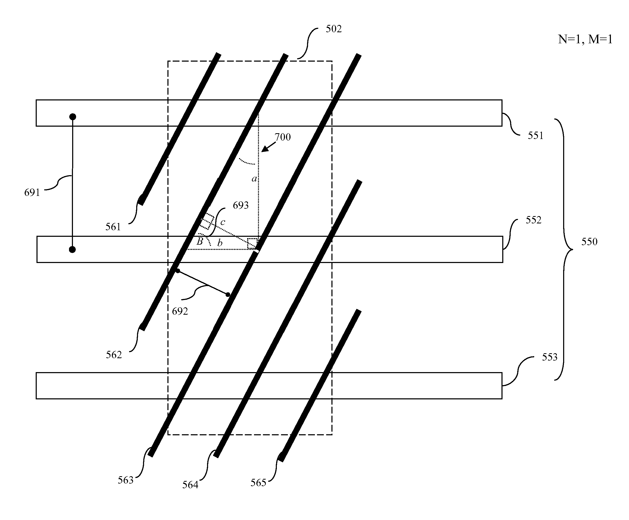
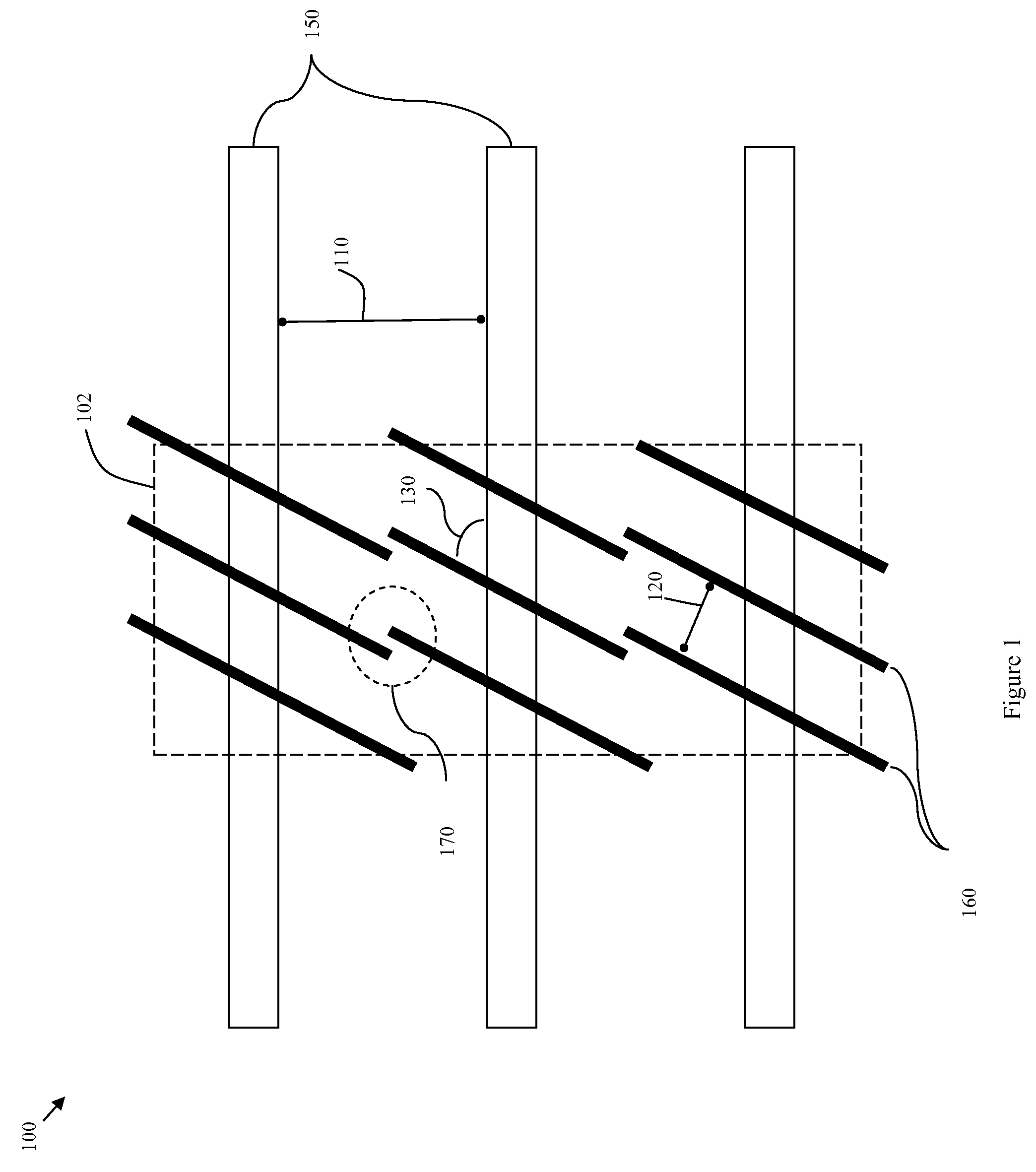
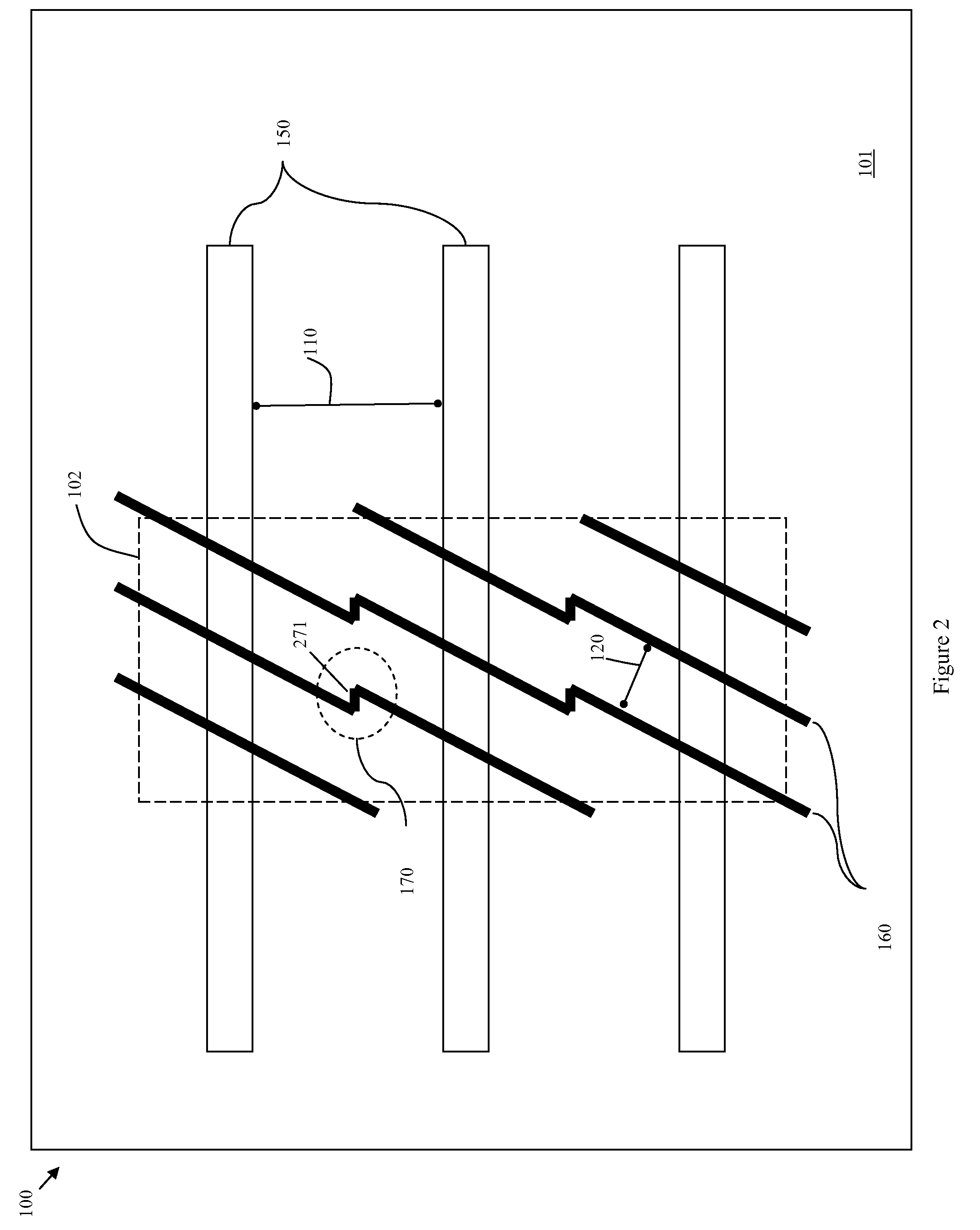
[0027]The embodiments of the invention and the various features and advantageous details thereof are explained more fully with reference to the non-limiting embodiments that are illustrated in the accompanying drawings and detailed in the following description. It should be noted that the features illustrated in the drawings are not necessarily drawn to scale. Descriptions of well-known components and processing techniques are omitted so as to not unnecessarily obscure the embodiments of the invention. The examples used herein are intended merely to facilitate an understanding of ways in which the embodiments of the invention may be practiced and to further enable those of skill in the art to practice the embodiments of the invention. Accordingly, the examples should not be construed as limiting the scope of the embodiments of the invention.

[0028]As mentioned above, non-planar field effect transistors (e.g., finFETs or trigate FETs formed with semiconductor fins) were developed to p...


PUM


Abstract

Disclosed are embodiments of semiconductor structure and a method of forming the semiconductor structure that simultaneously maximizes device density and avoids contacted-gate pitch and fin pitch mismatch, when multiple parallel angled fins are formed within a limited area on a substrate and then traversed by multiple parallel gates (e.g., in the case of stacked, chevron-configured, CMOS devices). This is accomplished by using, not a minimum lithographic fin pitch, but rather by using a fin pitch that is calculated as a function of a pre-selected contacted-gate pitch, a pre-selected fin angle and a pre-selected periodic pattern for positioning the fins relative to the gates within the limited area. Thus, the disclosed structure and method allow for the conversion of a semiconductor product design layout with multiple, stacked, planar FETs in a given area into a semiconductor product design layout with multiple, stacked, chevron-configured, non-planar FETs in the same area.

Description

BACKGROUND[0001]1. Field of the Invention[0002]The embodiments of the invention generally relate to integrated circuit structures and, more particularly, to an integrated circuits structure that incorporates multiple stacked chevron non-planar field effect transistors (FETs) and a method of forming the integrated circuit structure.[0003]2. Description of the Related Art[0004]As transistor design is improved and evolves, the number of different types of transistors continues to increase. Multi-gated non-planar metal oxide semiconductor field effect transistors (FETs), including dual-gate non-planar FETs (e.g., finFETs) and tri-gate non-planar FETs, were developed to provide scaled devices with higher drive currents and reduced short channel effects over planar FETs.[0005]Additionally, the mobility of charge carriers in FET channel regions can be optimized for different types of FETS (i.e., n-type FETs (NFETs) or p-type FETs (PFETs)) as a function of the semiconductor crystalline orie...

Claims


Application Information

Patent Timeline
Patent Type & Authority Patents(United States)
IPC IPC(8): H01L29/80
CPCH01L27/0207H01L21/823412H01L29/785
Inventor ANDERSON, BRENT A.BRYANT, ANDRESNOWAK, EDWARD J.
Owner GLOBALFOUNDRIES INC
Learn More