Bidirectional buffer circuit and signal level conversion circuit

a buffer circuit and signal level technology, applied in logic circuits, logic circuits coupling/interfaces with bidirectional operation, pulse techniques, etc., can solve the problems of reducing the chip size and the delay of the signal propagation, increasing the cost, and increasing the cos

Inactive Publication Date: 2010-11-23
KK TOSHIBA
View PDF12 Cites 2 Cited by
  • Summary
  • Abstract
  • Description
  • Claims
  • Application Information

AI Technical Summary

Problems solved by technology

Moreover, in the electronic devices and in the circuits, each power voltage of them is not always the same.
Using the directional signal, however, the buffer needs another long wire for the directional signal so that the cost increases.
However, such the apparatus complicates the buffer circuit and the level shifter, and therefore, the cost increases.
Moreover, the signal level conversion circuit reduces a chip size and a delay of the signal propagation.
However, also this disclosure example, the circuit becomes complex because of using a selective signal for switching the transmission direction of the signal and its structure becomes complex.

Method used


Image

  • Bidirectional buffer circuit and signal level conversion circuit
  • Bidirectional buffer circuit and signal level conversion circuit
  • Bidirectional buffer circuit and signal level conversion circuit

Examples


first embodiment

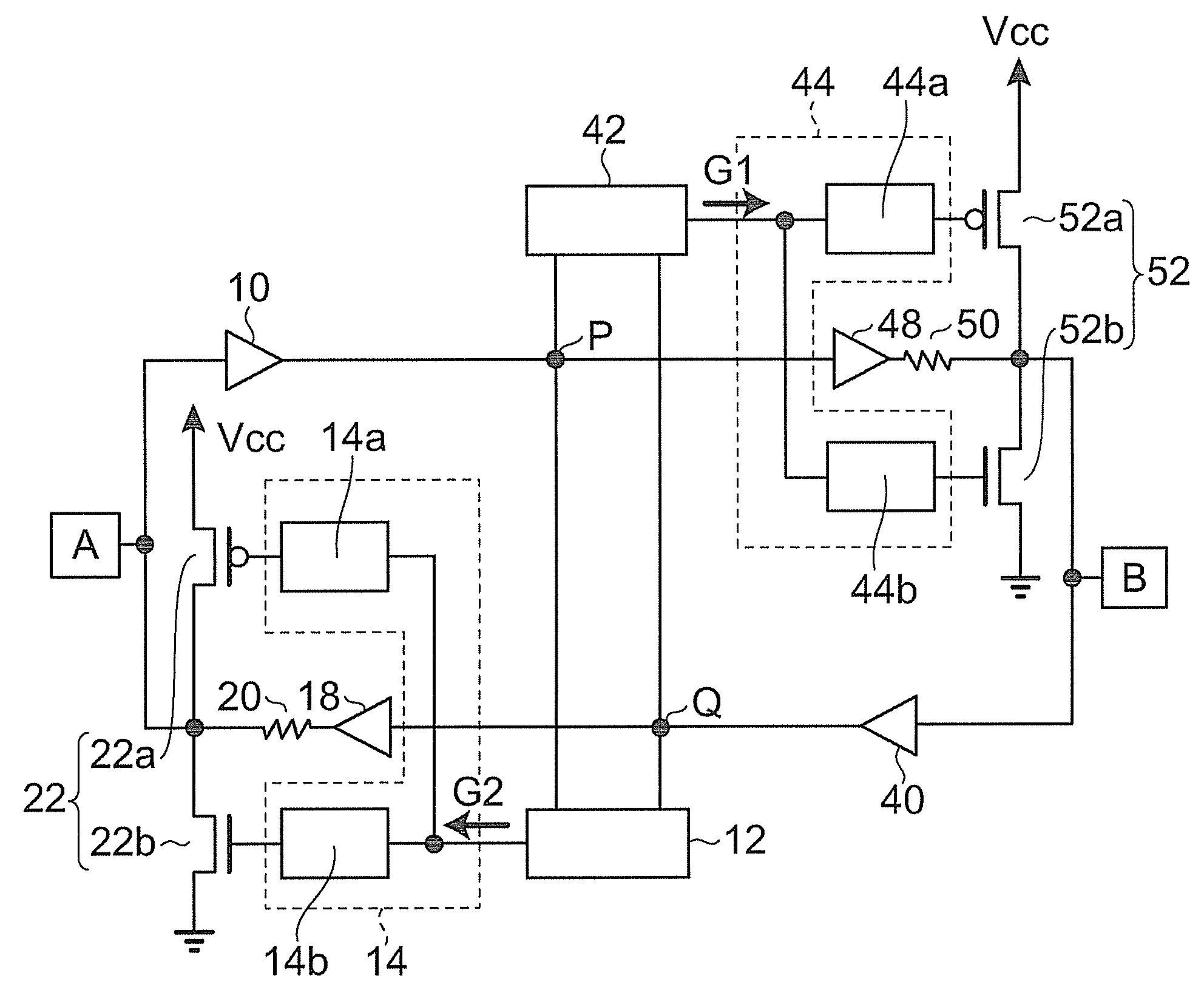
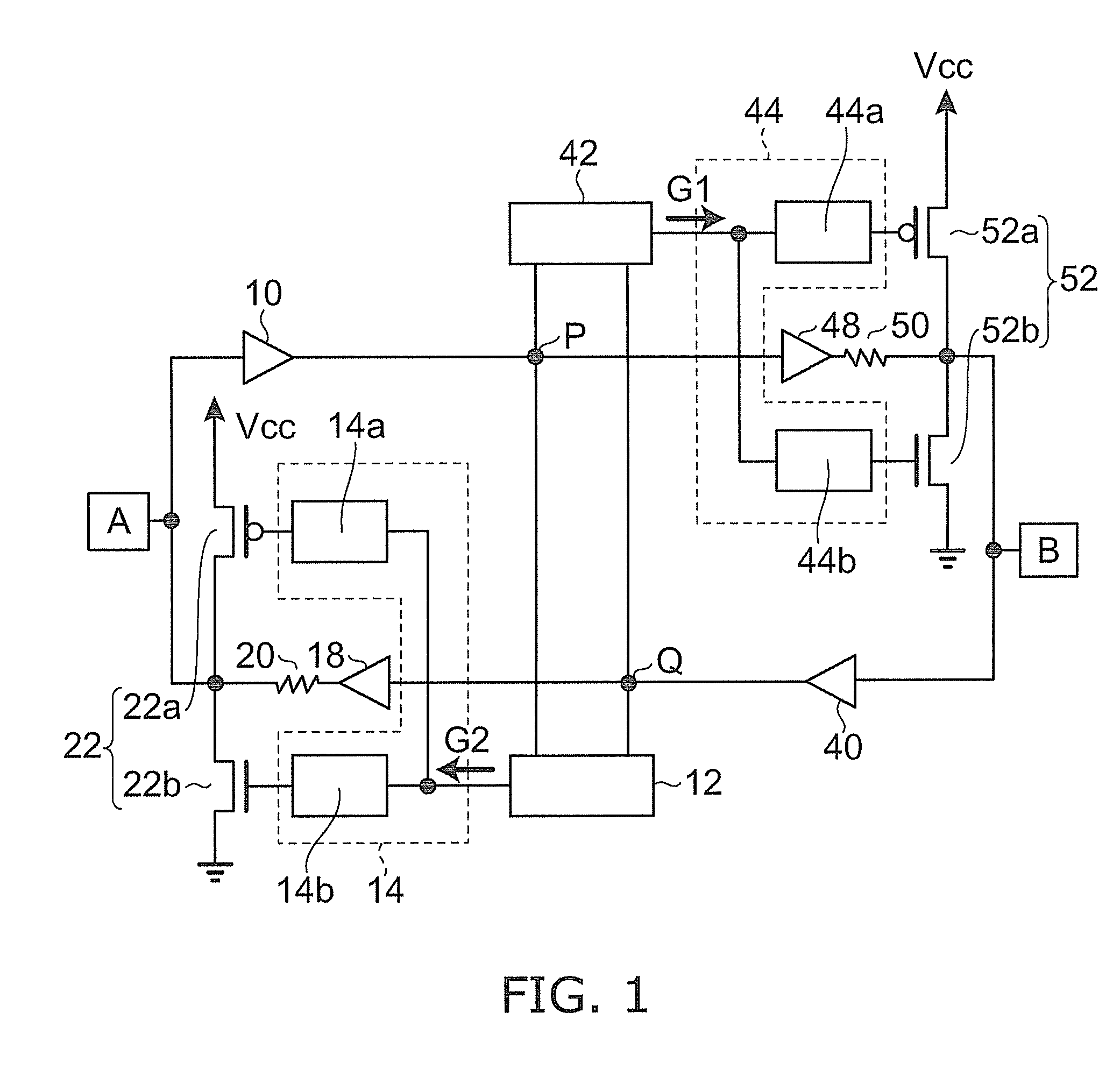
[0021]FIG. 1 shows a block diagram of a bidirectional buffer circuit according to the invention.

[0022]In this embodiment, the bidirectional buffer circuit mutually transmits data between a first terminal A and a second terminal B, and does not use a switching signal representing a transmission direction of a signal. A signal of a logical value of “0” or “1” is input from the terminal A to, for example, a first input buffer 10.

[0023]An output of the input buffer 10 is input to a first output buffer 48, and is output to the terminal B through a resistor 50. Moreover, the signal input to the terminal B is input to, for example, a second input buffer 40. An output of the input buffer 40 is input to a second output buffer 18, and output to the terminal A through a resistor 20. The buffer circuit may not the input buffers 10, 40, but when the input buffers are provided, the buffer circuit operates more stably.

[0024]As the buffer circuit comprises a data transmission loop having all of the...


PUM


Abstract

A bidirectional buffer circuit includes a first terminal, a second terminal, a first output buffer to which a signal from the first terminal is input and which outputs the signal to the second terminal, a first one-shot buffer control circuit outputting a first control signal according to an earlier arriving signal out of a signal from the first terminal and a signal from the second terminal, a first one-shot buffer temporarily driving the second terminal by the first control signal, a second output buffer to which a signal from the second terminal is input and which outputs the signal to the first terminal, a second one-shot buffer control circuit outputting a second control signal according to an earlier arriving signal out of a signal from the first terminal and a signal from the second terminal, and a second one-shot buffer temporarily driving the first terminal by the second control signal.

Description

CROSS-REFERENCE TO RELATED APPLICATIONS[0001]This application is based upon and claims the benefit of priority from the prior Japanese Patent Application No. 2008-145562, filed on Jun. 3, 2008; the entire contents of which are incorporated herein by reference.BACKGROUND OF THE INVENTION[0002]1. Field of the Invention[0003]This invention relates to a bidirectional buffer circuit and a signal level conversion circuit.[0004]2. Background Art[0005]In data transmission between electronic devices and between circuits, data transmitting and receiving are often performed alternately, and only one thereof is rarely performed. For example, in memory devices, stored data in a received address are transmitted to a sender in return. In this case, as the data transmitting and receiving are not often performed at the same time, bidirectional communication of transmitting and receiving the data is often performed with sharing one signal line. Thereby, the number of the signal lines can be small, an...

Claims


Application Information

Patent Timeline
Patent Type & Authority Patents(United States)
IPC IPC(8): H03K19/0175
CPCH03K19/0175H03K19/01759
Inventor HORI, CHIKAHIRO
Owner KK TOSHIBA
Why Eureka
Try Eureka