Semiconductor integrated circuit device
a technology of integrated circuits and semiconductors, applied in the direction of pulse techniques, transistors, basic electric elements, etc., can solve the problems of erroneous operation and difficulty in saying that the latch circuit in patent document 1 has sufficient toleran
- Summary
- Abstract
- Description
- Claims
- Application Information
AI Technical Summary
Benefits of technology
Problems solved by technology
Method used
Image

Examples
first example
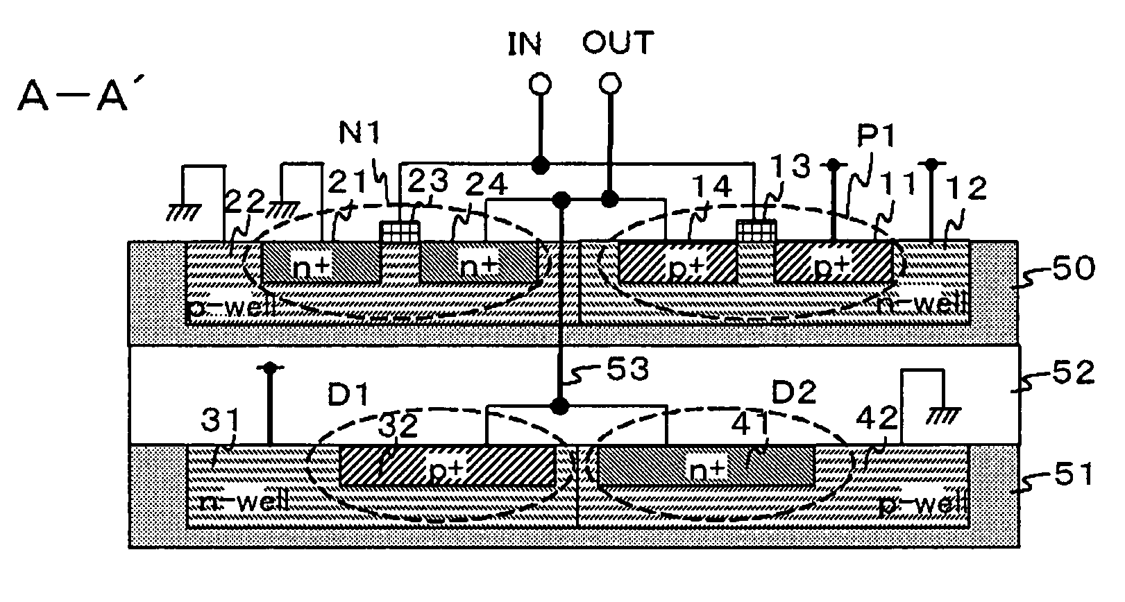
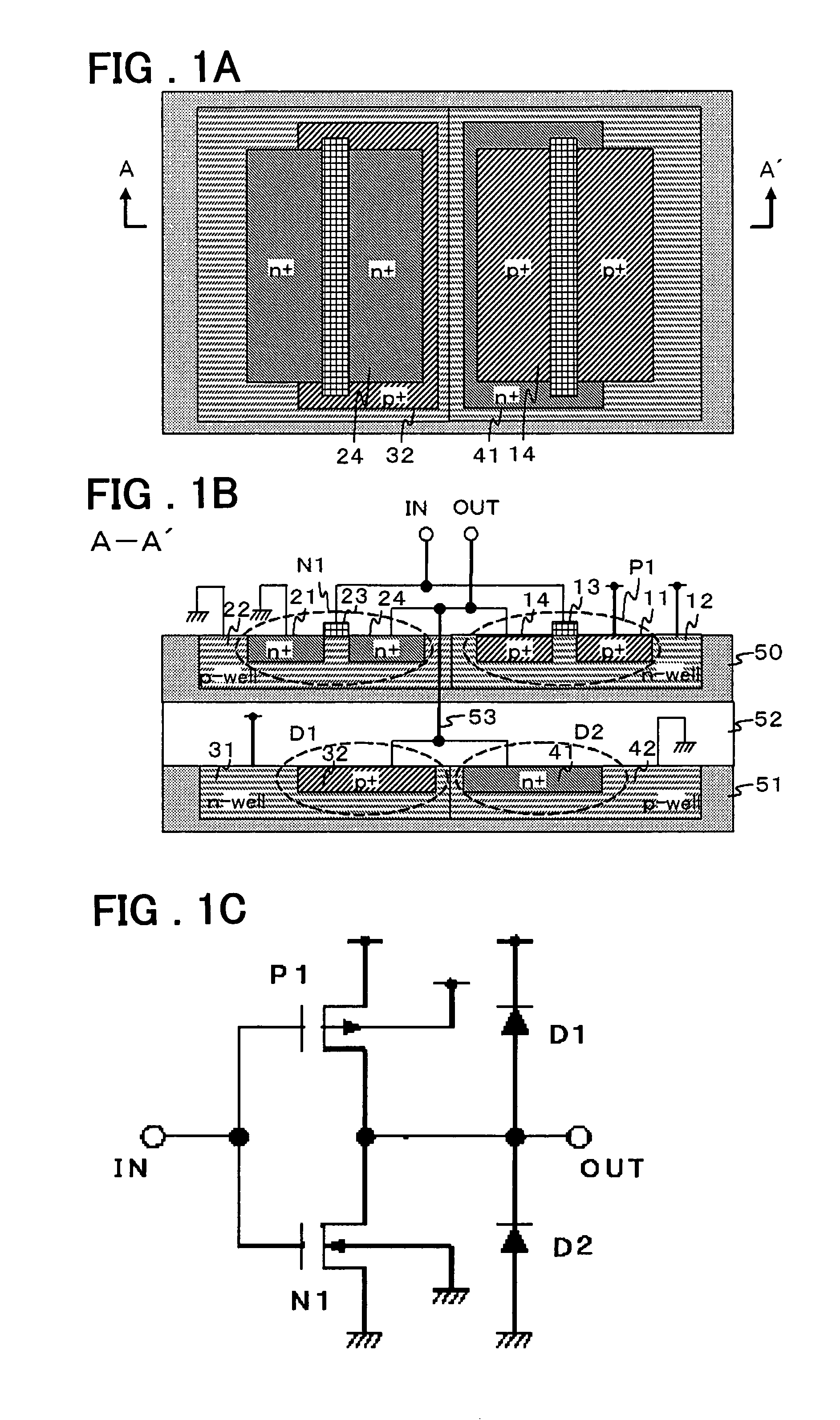
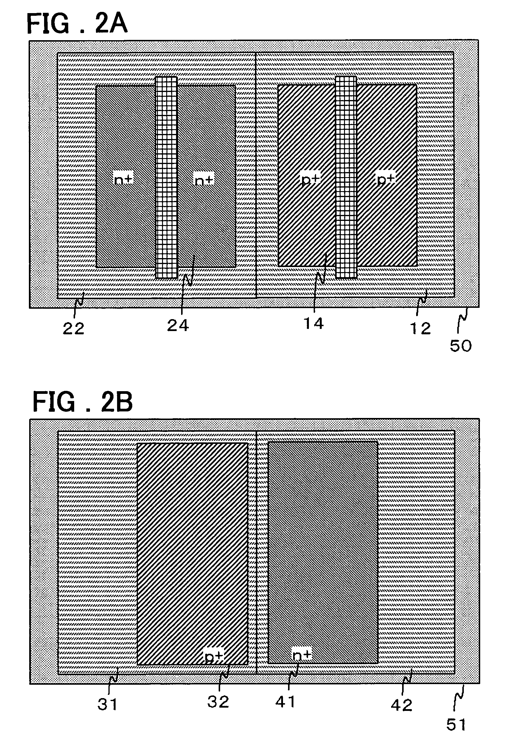
[0037]FIG. 1 includes diagrams showing a structure and a circuit of a semiconductor integrated circuit device according to a first example of the present invention. FIG. 1A is a plan view of the semiconductor integrated circuit device. FIG. 1B is a sectional view taken along a line A-A′ of the semiconductor integrated circuit device shown in FIG. 1A. FIG. 1C is a circuit diagram of the semiconductor integrated circuit device. Referring to FIGS. 1A, 1B and IC, the semiconductor integrated circuit device is an inverter circuit of the CMOS type, and includes a P-channel transistor P1, an N-channel transistor N1, and diodes D1 and D2. A source (a P+ diffusion layer 11) and a back gate (an n well 12) of the P-channel transistor P1 are connected to the power supply. A gate 13 of the P-channel transistor P1 is connected to an input terminal IN, and a drain (a p+ diffusion layer 14) of the P-channel transistor P1 is connected to an output terminal OUT. A source (an n+ diffusion layer 21) an...
second example
[0049]FIG. 6 is a circuit diagram of a semiconductor integrated circuit device according to a second example of the present invention. A logic circuit shown in FIG. 6 is a two-input NOR circuit of the CMOS type, and includes a P-channel transistor P2 and a P-channel transistor P3, an N-channel transistor N2 and an N-channel transistor N3, and the diodes D1 and D2. A source and a back gate of the P-channel transistor P2 is connected to the power supply, a gate of the P-channel transistor P2 is connected to an input terminal IN1, and a drain of the P-channel transistor P2 is connected to a source of the P-channel transistor P3. A back gate of the P-channel transistor P3 is connected to the power supply. A gate of the P-channel transistor P3 is connected to an input terminal IN2. A drain of the P-channel transistor P3 is connected to the output terminal OUT. A source and a back gate of each of the N-channel transistor N2 and the N-channel transistor N3 are grounded. A gate of the N-cha...
third example
[0053]FIG. 7 is a circuit diagram of a semiconductor integrated circuit device according to a third example of the present invention. A logic circuit shown in FIG. 7 is a two-input NAND circuit of the CMOS type, and includes a P-channel transistor P4 and a P-channel transistor P5, an N-channel transistor N4 and an N-channel transistor N5, and the diodes D1 and D2. A source and a back gate of each of the P-channel transistor P4 and the P-channel transistor P5 are connected to the power supply. A gate of the P-channel transistor P4 is connected to an input terminal IN3, and a gate of the P-channel transistor P5 is connected to an input terminal IN4. A drain of each of the P-channel transistor P4 and the P-channel transistor P5 is connected to the output terminal OUT. A source of the N-channel transistor N4 is connected to a drain of the N-channel transistor N5. A gate of the N-channel transistor N4 is connected to the input terminal IN3. A back gate of the N-channel transistor N4 is g...
PUM
 Abstract
Description
Claims
Application Information
 - R&D
- Intellectual Property
- Life Sciences
- Materials
- Tech Scout
- Unparalleled Data Quality
- Higher Quality Content
- 60% Fewer Hallucinations
Browse by: Latest US Patents, China's latest patents, Technical Efficacy Thesaurus, Application Domain, Technology Topic, Popular Technical Reports.
© 2025 PatSnap. All rights reserved.Legal|Privacy policy|Modern Slavery Act Transparency Statement|Sitemap|About US| Contact US: help@patsnap.com