


Quick Research
Generate reliable direction feasibility study reports for your R&D in just a few steps.

Technical Q&A
Discover and master advanced knowledge NOW. Basics, ideas, possibilities, all at once.

Find Solutions
As an expert in R&D theories, this can generate solutions to your technical problems instantly.

Evaluate Feasibility
Analyze your overall solution with one click, know your potential R&D risks in advance.

Monitor Landscape
Get weekly tech updates, stay abreast of the latest tech innovations and key insights.
Ferroelectric semiconductor storage device
a storage device and ferroelectric technology, applied in the field of ferroelectric semiconductor storage devices, can solve problems such as the reduction of ferroelectric memory size by hammering
- Summary
- Abstract
- Description
- Claims
- Application Information
AI Technical Summary
Benefits of technology
Problems solved by technology
Method used
Image

Examples
first embodiment
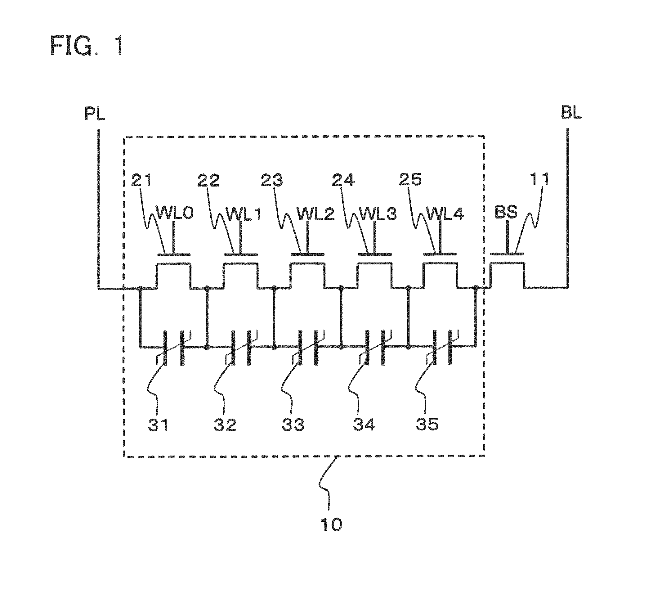
[0025]A first embodiment of the present invention will now be described below. This embodiment relates to a configuration of a ferroelectric memory of a FeRAM.
[0026]FIG. 1 is a circuit diagram illustrating a configuration of one block of ferroelectric memory cells according to the first embodiment. In this embodiment, odd numbers of ferroelectric memory cells are included in one block, one end of which is connected to a selection transistor.
[0027]Specifically, a ferroelectric memory block 10 is formed by the following ferroelectric memory cells that are connected in series: a ferroelectric memory cell having a transistor 21 connected in parallel to both ends of a ferroelectric capacitor 31; a ferroelectric memory cell having a transistor 22 connected in parallel to both ends of a ferroelectric capacitor 32; a ferroelectric memory cell having a transistor 23 connected in parallel to both ends of a ferroelectric capacitor 33; a ferroelectric memory cell having a transistor 24 connecte...
second embodiment
[0037]A second embodiment of the present invention will now be described below. This embodiment relates to a configuration of a ferroelectric memory of a FeRAM.
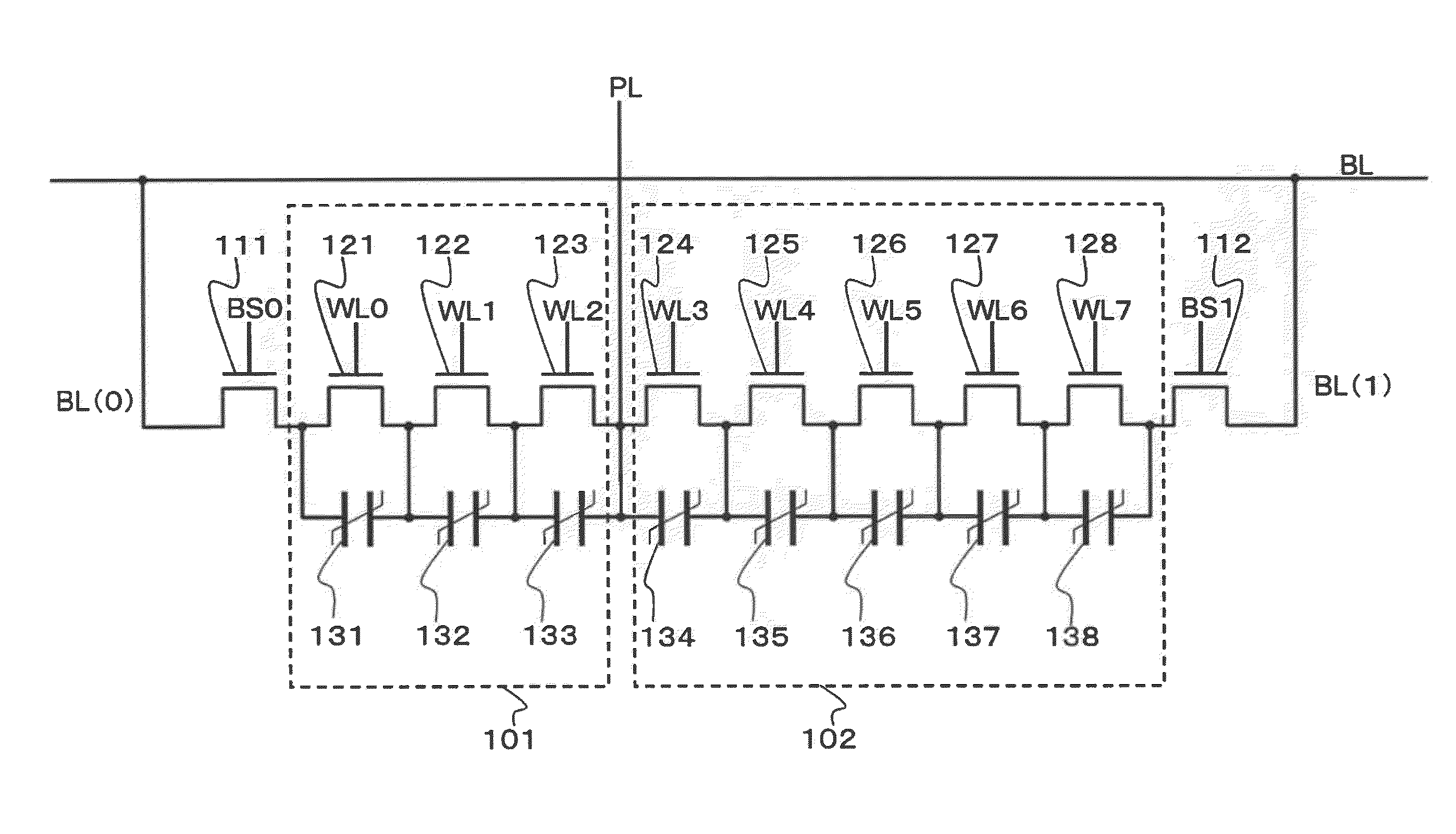
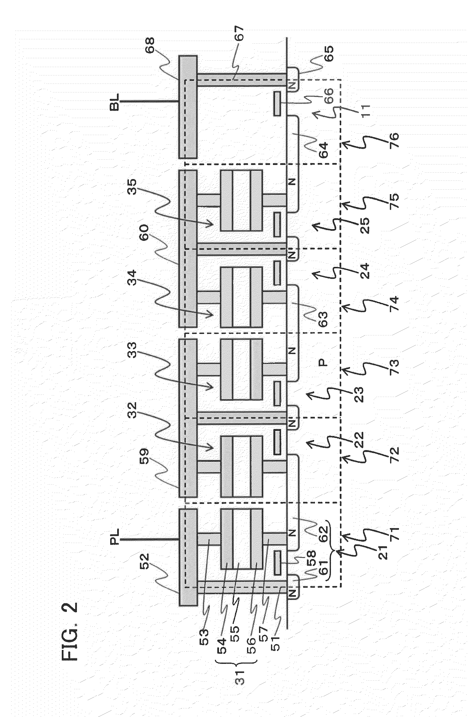
[0038]FIG. 4 is a circuit diagram illustrating a configuration of one block in the ferroelectric memory according to the second embodiment. This embodiment comprises one ferroelectric memory block having a first block and a second block connected in series. Each of the first and second blocks has odd numbers of ferroelectric memory cells connected in series, respectively. Thus, the one ferroelectric memory block includes even numbers of ferroelectric memory cells.
[0039]Specifically, a first block 101 is formed by the following ferroelectric memory cells that are connected in series: a ferroelectric memory cell having a transistor 121 connected to both ends of a ferroelectric capacitor 131; a ferroelectric memory cell having a transistor 122 connected to both ends of a ferroelectric capacitor 132; and a ferroelectric memory ce...
third embodiment
[0063]A third embodiment of the present invention will now be described below.
[0064]FIG. 9 is a circuit diagram illustrating a configuration of ferroelectric memory cells according to the third embodiment. This embodiment combines two blocks, each of which includes odd numbers of ferroelectric memory cells, wherein a respective selection transistor is connected to one end of each block.
[0065]Specifically, the ferroelectric memory according to this embodiment includes two ferroelectric memory blocks 210 and 310. The ferroelectric memory block 210 has the following ferroelectric memory cells that are connected in series: a ferroelectric memory cell having a transistor 221 connected in parallel to both ends of a ferroelectric capacitor 231; a ferroelectric memory cell having a transistor 222 connected in parallel to both ends of a ferroelectric capacitor 232; a ferroelectric memory cell having a transistor 223 connected in parallel to both ends of a ferroelectric capacitor 233; a ferro...
PUM
 Abstract
Description
Claims
Application Information
 - R&D Engineer
- R&D Manager
- IP Professional
- Industry Leading Data Capabilities
- Powerful AI technology
- Patent DNA Extraction
Browse by: Latest US Patents, China's latest patents, Technical Efficacy Thesaurus, Application Domain, Technology Topic, Popular Technical Reports.
© 2024 PatSnap. All rights reserved.Legal|Privacy policy|Modern Slavery Act Transparency Statement|Sitemap|About US| Contact US: help@patsnap.com