Wireless IC device and electronic device
a technology of electronic devices and wires, applied in the direction of resonant antennas, high frequency circuit adaptations, instruments, etc., can solve the problems of increasing size and increasing cost, and achieve the effect of easy impedance matching
- Summary
- Abstract
- Description
- Claims
- Application Information
AI Technical Summary
Benefits of technology
Problems solved by technology
Method used
Image
Examples
first preferred embodiment
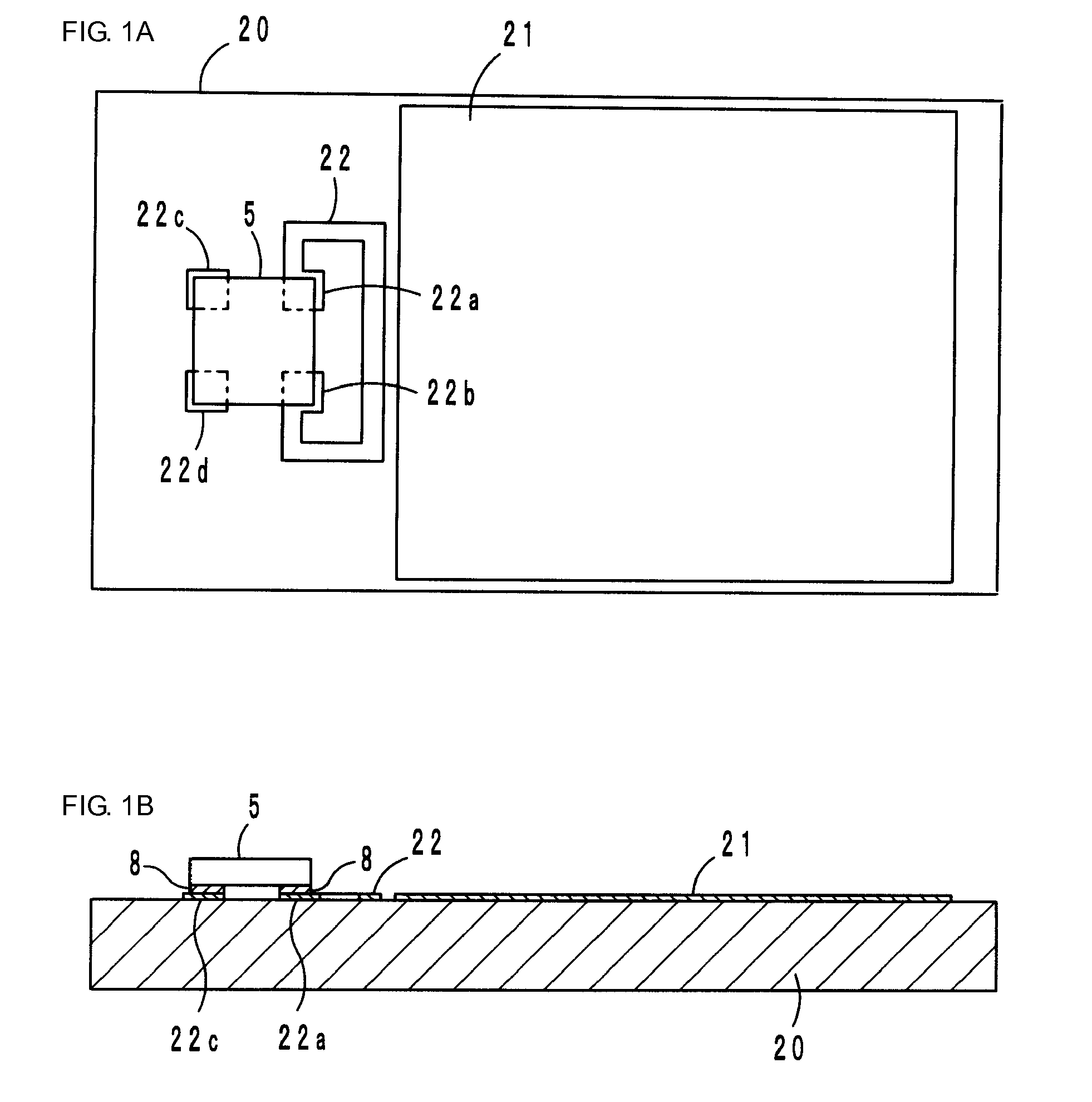
FIGS. 1A and 1B and FIG. 2
[0028]FIGS. 1A and 1B show a wireless IC device according to a first preferred embodiment of the present invention. This wireless IC device includes a wireless IC chip 5 for processing a transmission / reception signal of a predetermined frequency, a printed wiring circuit board 20 on which the wireless IC chip 5 is mounted, and a ground electrode 21 and a substantially loop-shaped electrode 22 that are disposed on the circuit board 20. The ground electrode 21 and the substantially loop-shaped electrode 22 are provided on the principal surface of the printed wiring circuit board 20 through application of a conductive paste, etching of a metal foil provided on the circuit board 20, or the like.
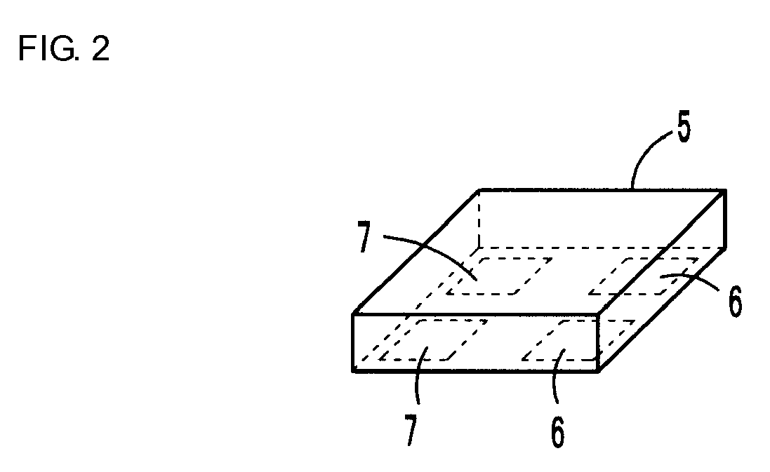
[0029]The wireless IC chip 5 preferably includes a clock circuit, a logic circuit, a memory circuit, and the like, and stores necessary information. As shown in FIG. 2, the wireless IC chip 5 has input / output terminal electrodes 6, 6 and mounting terminal electrodes 7, 7...
second preferred embodiment
FIGS. 3A and 3B
[0034]FIGS. 3A and 3B show a wireless IC device according to a second preferred embodiment of the present invention. This wireless IC device is of basically the same configuration as that of the above-mentioned first preferred embodiment, except that the ground electrode 21 and the substantially loop-shaped electrode 22 are disposed on the back surface of the printed wiring circuit board 20. Connection electrodes 24a to 24d are disposed on the front surface of the circuit board 20. The connection electrodes 24a, 24b are electrically connected to the opposite ends of the substantially loop-shaped electrode 22 via a via-hole conductor 23. The connection electrodes 24a to 24d correspond to the connection electrodes 22a to 22d shown in FIGS. 1A and 1B, and are electrically connected to the terminal electrodes 6, 6, 7, 7 (see FIG. 2) of the wireless IC chip 5 via the metal bump 8.
[0035]The coupling state between the ground electrode 21 and the substantially loop-shaped ele...
third preferred embodiment
FIGS. 4A to 4C
[0036]FIGS. 4A to 4C show a wireless IC device according to a third preferred embodiment of the present invention. In this wireless IC device, a substantially loop-shaped electrode 25 is defined by connection electrodes 25a, 25b provided on the front surface of the printed wiring circuit board 20, via-hole conductors 28, 28, and an internal electrode 29. The substantially loop-shaped electrode 25 is coupled by an electric field to the ground electrode 21 provided on the back surface of the circuit board 20. The connection electrodes 25a, 25b and the connection electrodes 25c, 25d are electrically connected to the terminal electrodes 6, 6, 7, 7 (see FIG. 2) of the wireless IC chip 5 via the metal bump 8.
[0037]The substantially loop-shaped electrode 25 is arranged substantially perpendicular and in close proximity to the ground electrode 21, and the two electrodes are coupled to each other by an electric field. That is, the substantially loop-shaped electrode 25 produces...
PUM
 Abstract
Description
Claims
Application Information
 - R&D
- Intellectual Property
- Life Sciences
- Materials
- Tech Scout
- Unparalleled Data Quality
- Higher Quality Content
- 60% Fewer Hallucinations
Browse by: Latest US Patents, China's latest patents, Technical Efficacy Thesaurus, Application Domain, Technology Topic, Popular Technical Reports.
© 2025 PatSnap. All rights reserved.Legal|Privacy policy|Modern Slavery Act Transparency Statement|Sitemap|About US| Contact US: help@patsnap.com


