Light-emitting display device with light-blocking layer and manufacturing method thereof

a technology of light-emitting display device and manufacturing method, which is applied in the manufacture of electric discharge tube/lamp, discharge tube luminescnet screen, instruments, etc., can solve problems such as property changes, and achieve favorable performance, favorable light-blocking property, and favorable performan

Inactive Publication Date: 2010-11-09
SEMICON ENERGY LAB CO LTD
View PDF17 Cites 16 Cited by
  • Summary
  • Abstract
  • Description
  • Claims
  • Application Information

AI Technical Summary

Benefits of technology

[0012]In addition to the structure above, light extraction efficiency can be improved by providing reflectivity for each of the electrodes formed using a material having a light-blocking property, which is further preferable.
[0020]The reason why light leaks in a horizontal direction to the substrate is that, in a structure around the monitoring element, one or more insulating layers having a light-transmitting property are formed between a film used as a light-blocking layer and a pixel electrode, and light emitted from a light emitting layer of the monitoring element passes through the insulating layer to leak in the horizontal direction to the substrate. Therefore, according to the present invention, an insulating layer formed in a region overlapping a light emitting layer of a monitoring element is removed by patterning so as to form a depression; a light emitting element including the light emitting layer, a pixel electrode, and a counter electrode is formed in this region; and the light emitting layer is sealed with a light-blocking layer and the counter electrode. By applying such a structure to a monitoring element in a monitoring element portion, a route through which light emitted from the light emitting layer leaks can be eliminated not only for a vertical direction but also a horizontal direction to a substrate. Therefore, a favorable light-blocking property can be obtained even when the monitoring element portion and the pixel portion have no distance between each other.
[0021]According to the present invention, light-blocking around the monitoring element can be performed favorably without providing a distance between the pixel portion and the monitoring element portion and without extending the light-blocking layer in the horizontal direction to the substrate. As a result, the monitoring element portion can be arranged in a region closer to the pixel portion, therefore, characteristics of EL elements in the pixel portion and the monitoring element portion can be made closer to each other and the luminance correction and the like can be performed more favorably. Because of these two points, favorable display that is not affected by leak light of the monitoring element and favorable display due to the more accurate luminance correction can be obtained.

Problems solved by technology

On the other hand, an organic EL element has a problem in that changes in the properties, such as a reversible change associated with an environmental temperature change and an irreversible change like element deterioration caused by moisture or the like, specifically, are larger than those of an inorganic EL element.

Method used


Image

  • Light-emitting display device with light-blocking layer and manufacturing method thereof
  • Light-emitting display device with light-blocking layer and manufacturing method thereof
  • Light-emitting display device with light-blocking layer and manufacturing method thereof

Examples


embodiment mode 1

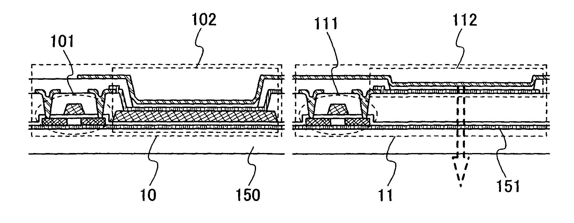
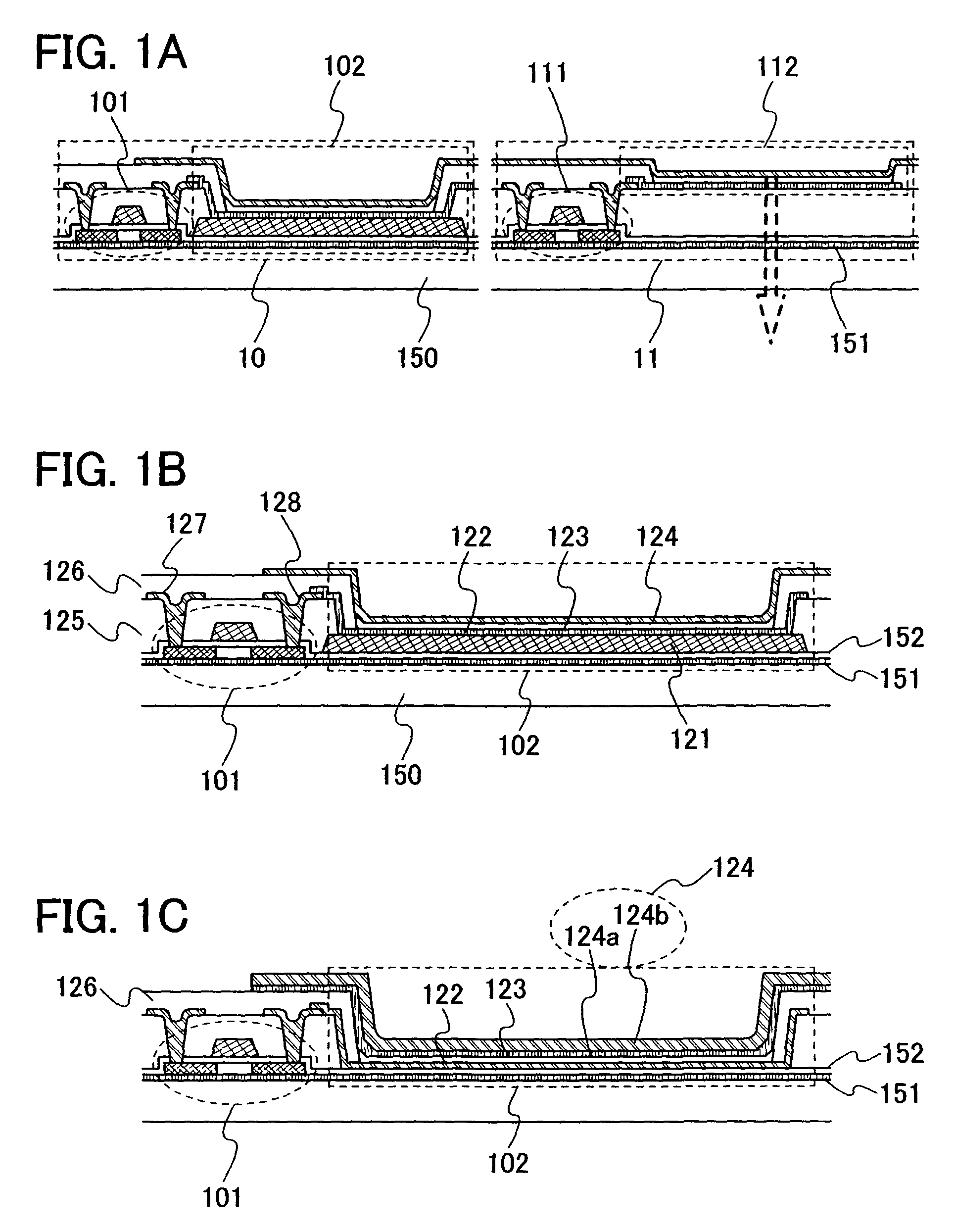
[0034]FIG. 1A is a view showing a mode of implementing the present invention. In a region indicated by a dotted frame 10, a TFT 101 and a monitoring element portion including a monitoring element 102 which is a light emitting element and the like are provided. In a region indicated by a dotted frame 11, a TFT 111 and a pixel portion including a light emitting element 112 and the like are provided. These are formed over a substrate 150 which is formed using a material having a light-transmitting property, such as glass or plastic. A base film 151, a gate insulating film 152, and the like may be formed over the substrate 150. Furthermore, although the peripheral circuit 200 which is shown in FIG. 2A for the related art is not shown in FIGS. 1A to 1C, it may be provided in the vicinity of the monitoring element portion or the pixel portion.

[0035]FIG. 1B is an enlarged view of the monitoring element portion shown in FIG. 1A. Concurrently with forming the TFT 101, a light-blocking layer ...

embodiment mode 2

[0041]FIGS. 3A to 3D show a different mode of the structure shown in FIG. 1B. In the top emission case, the pixel electrode formed using a material having reflectivity or a light-blocking property and the counter electrode including the light-blocking layer surround the light emitting layer in the horizontal direction as well (as shown in FIG. 1C). In the bottom emission case, however, the structure shown in FIG. 1B may not sufficiently prevent leak light since only the pixel electrode formed using a material having a light transmitting property surrounds the light emitting layer in the horizontal direction.

[0042]As the countermeasure against this, there is a method in which a structure using a material having a light-blocking property is formed in the horizontal direction. Hereinafter, the method will be described in detail referring to FIGS. 3A to 3D.

[0043]FIGS. 3A to 3C show structures of the monitoring element portion seen from the top, and a cross-sectional structure along line...

embodiment 1

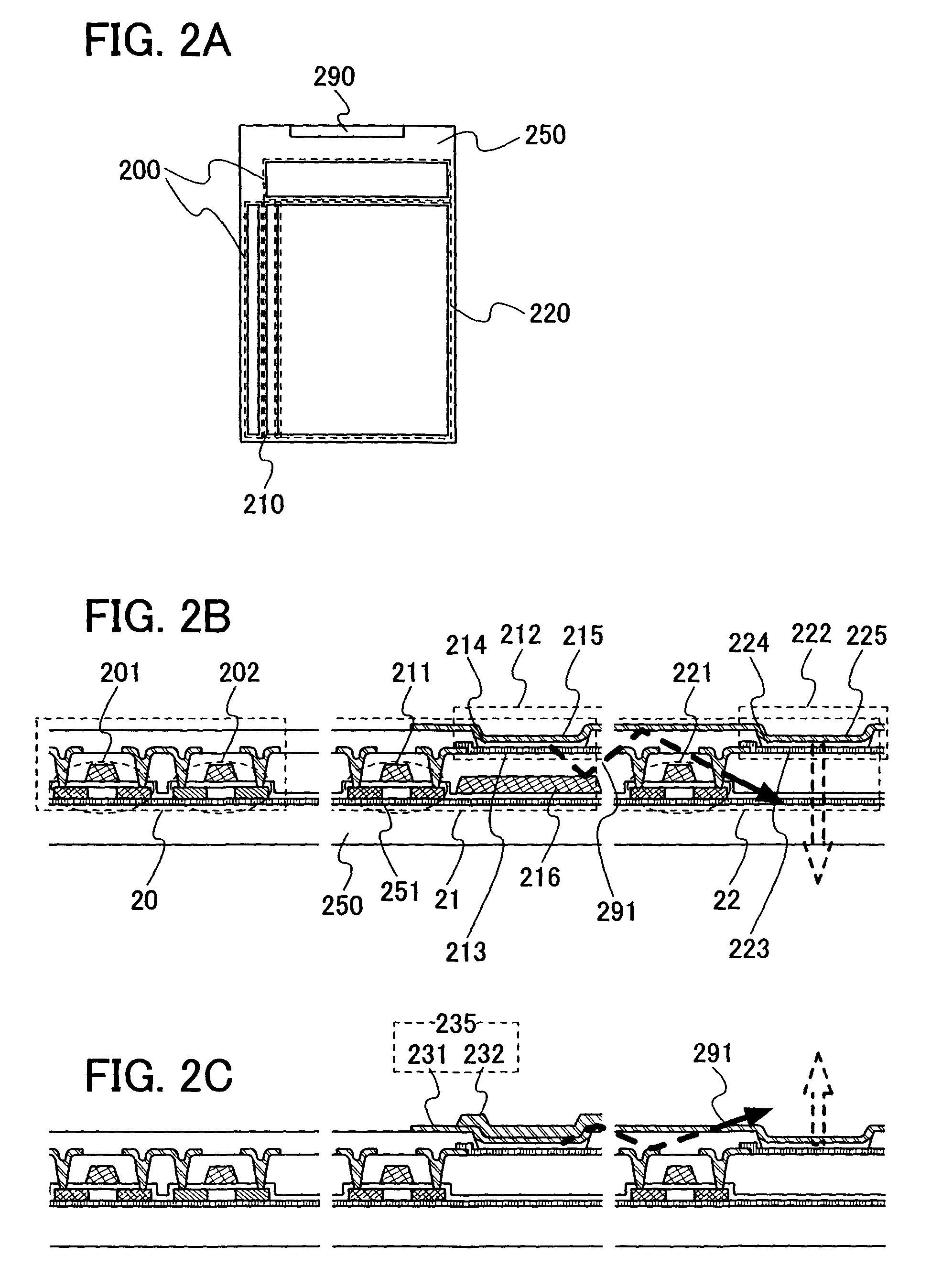
[0056]Formation of a display device having the structure of the present invention will be described with reference to drawings. Here, each step will be described in order, using FIGS. 4A and 4B. Although FIGS. 4A and 4B show a cross-section of only a monitoring element portion, TFTs, a wiring and the like constituting a peripheral circuit may be formed concurrently with a step of forming a TFT included in the monitoring element portion, and a pixel portion may be formed in the same way; therefore, they are not illustrated here.

[0057]FIG. 4A shows a cross-sectional view of a bottom emission display device, and FIG. 4B shows a cross-sectional view of a top emission display device. The same reference numerals are used for the structures common to the two views. Hereinafter, the description will be made with reference to the two views.

[0058]As a substrate 401 having an insulating surface, a glass substrate, a quartz substrate, or the like can be used. A substrate formed of a synthetic r...


PUM


Abstract

In a display device with a pixel constituted using an EL element or the like, leak light from a monitoring element that is provided for correcting changes in the properties of the element due to the temperature change, deterioration, or the like is effectively suppressed. The display device has a structure in which an insulating layer is formed over a substrate and a plurality of light emitting elements each of which has a light emitting layer interposed between a first electrode and a second electrode are formed over the insulating layer. Furthermore, at least part of the plurality of light emitting elements has a structure in which an opening is formed in the insulating layer, and the light emitting layer is formed in the opening region of the insulating layer.

Description

BACKGROUND OF THE INVENTION[0001]1. Field of the Invention[0002]The present invention relates to a display device and a manufacturing method of the same.[0003]2. Description of the Related Art[0004]In recent years, development toward the practical use of an EL display, which uses an electroluminescence element (hereinafter referred to as an EL element) for a pixel portion, has been promoted. Especially an EL display using an organic EL element can be operated with a driving voltage equivalent to that of a liquid crystal element which is mainly used in conventional flat panel displays, and the driving voltage is lower than that of an inorganic EL element. Specifically, compared to a liquid crystal display, an EL display device using an organic EL element is self-luminous, thus does not require a backlight, and its color reproducibility is high. Therefore, it is highly expected to be a key technology to the next-generation flat panel display.[0005]On the other hand, an organic EL elem...

Claims


Application Information

Patent Timeline
Patent Type & Authority Patents(United States)
IPC IPC(8): H01L51/50H01L51/52H01L51/56
CPCG09G3/3258G09G2320/029G09G2330/021H10K50/125H10K59/122H01L31/02164H10K2101/90
Inventor TANADA, YOSHIFUMI
Owner SEMICON ENERGY LAB CO LTD
Why Eureka
Try Eureka