
Active terahertz metamaterial devices

a technology of metamaterials and active terahertz, which is applied in the direction of resonant antennas, semiconductor lasers, instruments, etc., can solve the problems of lagging behind the techniques to control and manipulate thz waves, and achieve the effects of increasing the capacitance of the gaps in the resonator, increasing the resonant response, and reducing the cost of resonant measuremen

Active Publication Date: 2010-11-02
NAT TECH & ENG SOLUTIONS OF SANDIA LLC
View PDF16 Cites 51 Cited by
  • Summary
  • Abstract
  • Description
  • Claims
  • Application Information

AI Technical Summary

Benefits of technology

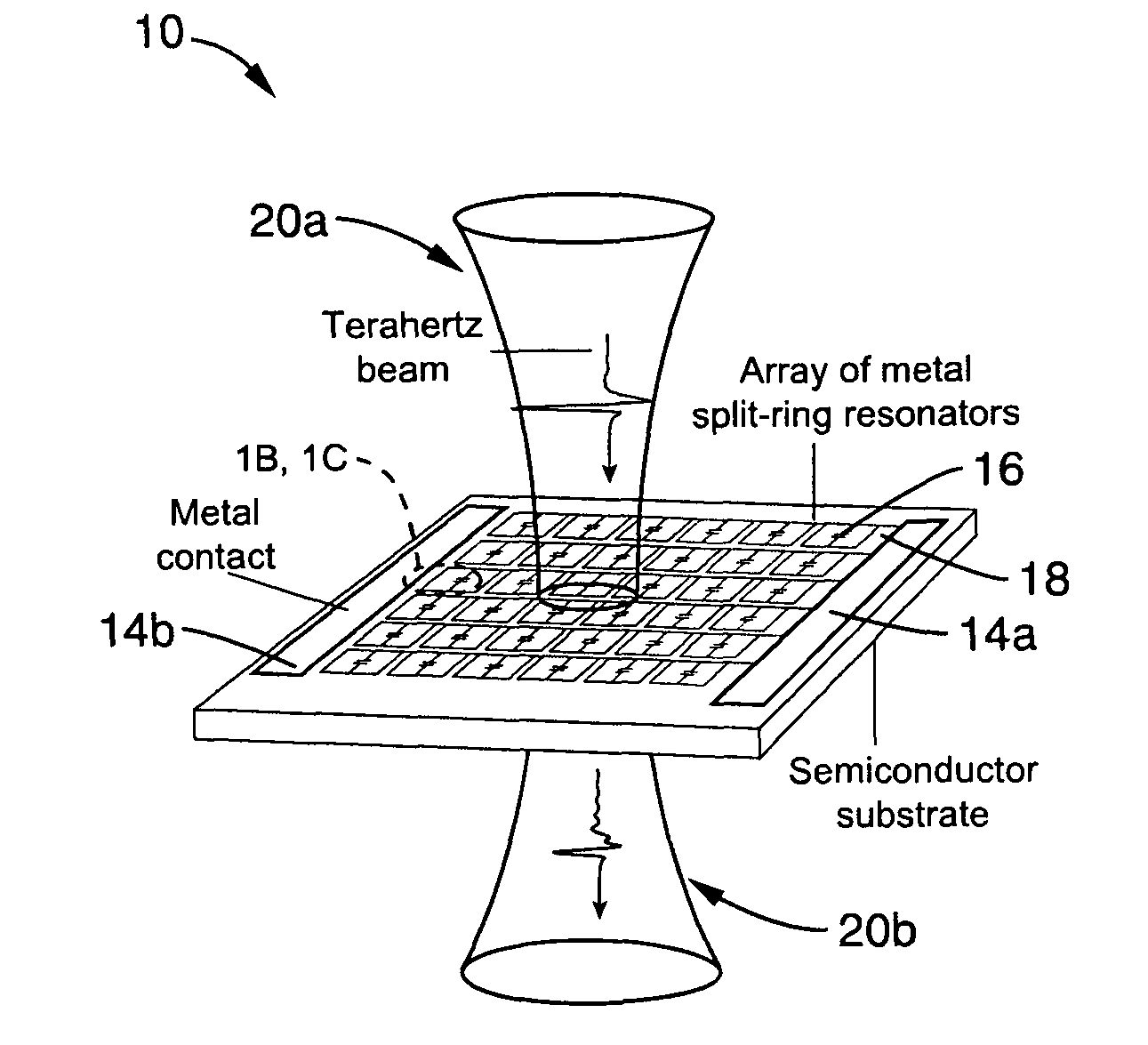
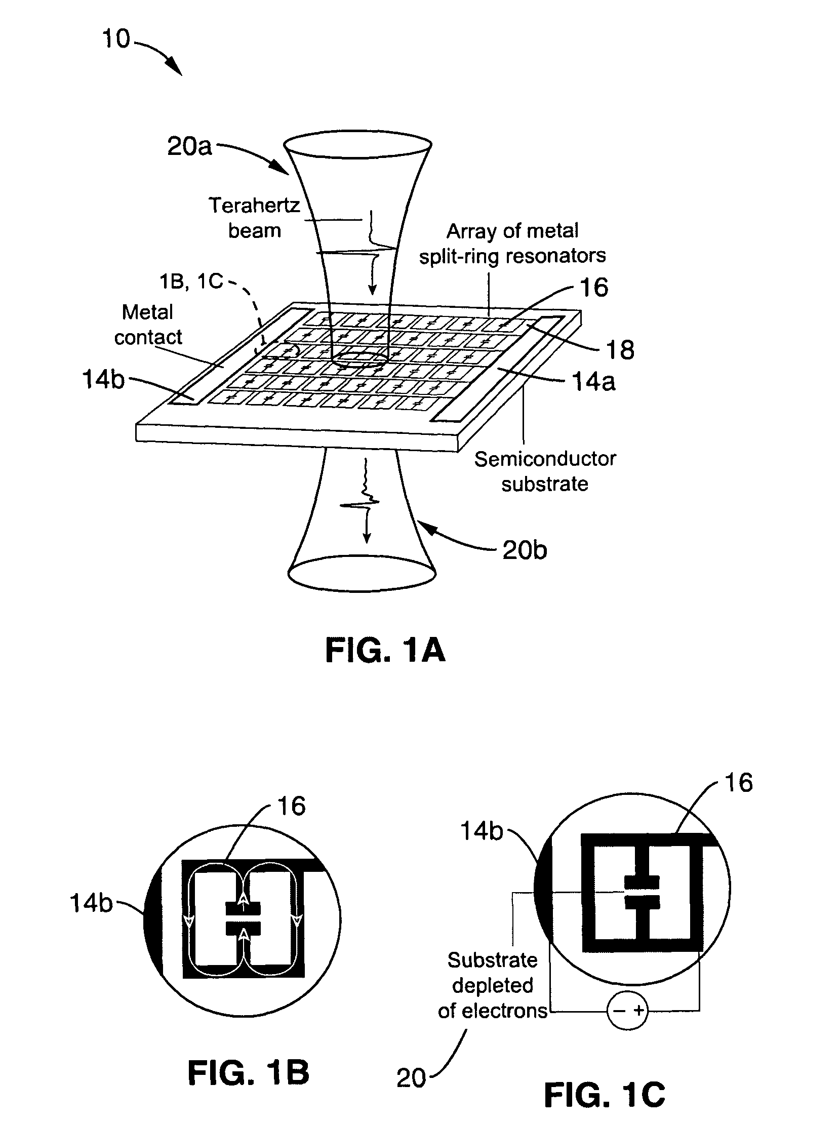
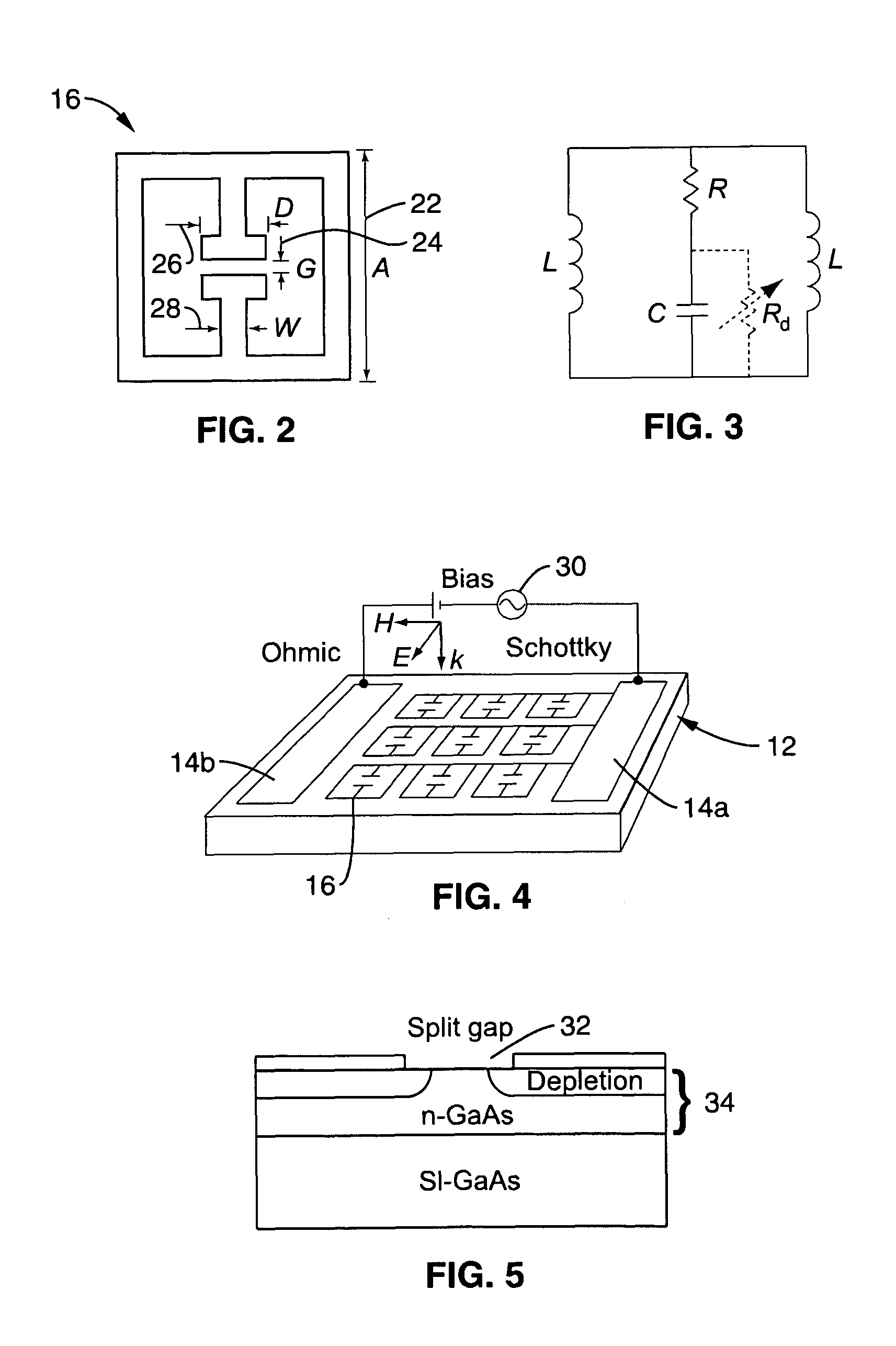
[0017]The gap in each split-ring resonators can operate to drive the capacitance toward zero, and thus dampens resonant response, when sufficient electrons are present near the gap. Alternatively, capacitance of the gaps in the resonators increases, and thus increases resonant response, in response to the depletion of electrons from the gap.
[0018]The modulator provides excellent transmissivity ratio of approximately 0.5, and can be operated at room temperature. The resonators in the modulator provide a resonant response although without a negative refractive index. At frequencies near the characteristic frequency of the resonant electron flow, the values of permittivity (∈) and permeability (μ) vary over a wide range in response to small changes in frequency. This modulator is easy to fabricate with a substrate comprising a sufficiently thin layer of semiconductor to allow the passage of a substantial portion of the terahertz radiation during portions of resonant cycles within the split-ring resonators. Preferably, the substrate comprises a lightly-doped semiconductor material.

Problems solved by technology

However, techniques to control and manipulate THz waves are lagging behind.

Method used


Image

  • Active terahertz metamaterial devices
  • Active terahertz metamaterial devices
  • Active terahertz metamaterial devices

Examples


Embodiment Construction

[0075]Referring more specifically to the drawings, for illustrative purposes the present invention is embodied in the apparatus generally shown in FIG. 1 through FIG. 60 and FIG. 62 through FIG. 70. It will be appreciated that the apparatus may vary as to configuration and as to details of the parts, and that the method may vary as to the specific steps and sequence, without departing from the basic concepts as disclosed herein.

[0076]The following description is provided in a number of sections. As these sections are based on separate documents and articles, the descriptions overlap in many areas.

[0077]1. Introduction to Terahertz MM Modulators

[0078]Discussed in this introduction are the use of resonators (e.g., metal) for creating a material with tunable responses to an applied voltage. When combined with a semiconductor substrate, these materials can be used to control technologically promising terahertz radiation.

[0079]Electromagnetic radiation with frequencies lying between the ...


PUM


Abstract

Metamaterial structures are taught which provide for the modulation of terahertz frequency signals. Each element within an array of metamaterial (MM) elements comprises multiple loops and at least one gap. The MM elements may comprise resonators with conductive loops and insulated gaps, or the inverse in which insulated loops are present with conductive gaps; each providing useful transmissive control properties. The metamaterial elements are fabricated on a semiconducting substrate configured with a means of enhancing or depleting electrons from near the gaps of the MM elements. An on to off transmissivity ratio of about 0.5 is achieved with this approach. Embodiments are described in which the MM elements incorporated within a Quantum Cascade Laser (QCL) to provide surface emitting (SE) properties.

Description

CROSS-REFERENCE TO RELATED APPLICATIONS[0001]This application is a 35 U.S.C. §111 (a) continuation of, co-pending PCT international application serial number PCT / US2007 / 082023, filed on Oct. 19, 2007, incorporated herein by reference in its entirety, which claims priority from U.S. provisional application Ser. No. 60 / 853,503 filed on Oct. 19, 2006, incorporated herein by reference in its entirety. Priority is claimed to each of the listed applications.STATEMENT REGARDING FEDERALLY SPONSORED RESEARCH OR DEVELOPMENT[0002]This invention was made with Government support under Contract No. DE-AC52-06NA25396 awarded by the U.S. Department of Energy. The Government has certain rights in this invention.INCORPORATION-BY-REFERENCE OF MATERIAL SUBMITTED ON A COMPACT DISC[0003]Not ApplicableNOTICE OF MATERIAL SUBJECT TO COPYRIGHT PROTECTION[0004]A portion of the material in this patent document is subject to copyright protection under the copyright laws of the United States and of other countri...

Claims


Application Information

Patent Timeline
Patent Type & Authority Patents(United States)
IPC IPC(8): H01S5/00H01Q15/22
CPCH03C7/027G02F1/015H01Q15/0086
Inventor CHEN, HOUTONGPADILLA, WILLIE JOHNAVERITT, RICHARD DOUGLASO'HARA, JOHN F.LEE, MARK
Owner NAT TECH & ENG SOLUTIONS OF SANDIA LLC
Learn More