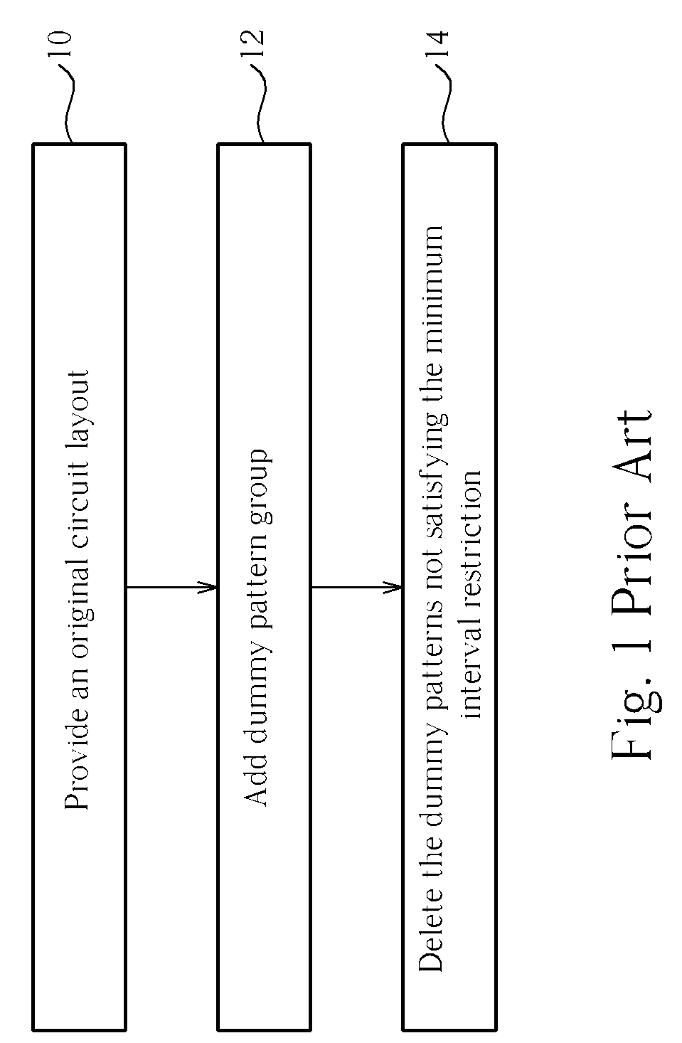
Computer readable medium having multiple instructions stored in a computer readable device
a computer readable medium and storage device technology, applied in computer aided design, total factory control, instruments, etc., can solve the problems of inability to improve the design for reliability/manufacturability cannot be improved, and the bottleneck becomes harder and harder to overcome. to overcome the bottleneck, the effect of improving the design for reliability/manufacturability
- Summary
- Abstract
- Description
- Claims
- Application Information
AI Technical Summary
Benefits of technology
Problems solved by technology
Method used
Image

Examples
first embodiment
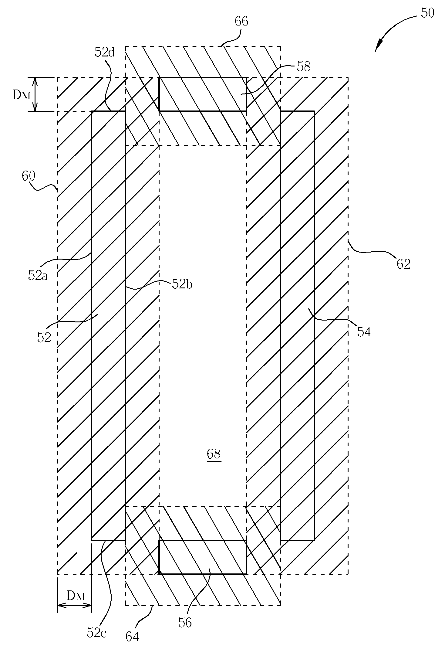
[0034]Please refer to FIGS. 5-9, which are schematic diagrams of the method for arranging virtual patterns through instructions executed by a computer readable medium comprising multiple instructions stored in a computer readable device according to the present invention. First, as shown in FIG. 5, a semiconductor layout 50 is provided, which comprises circuit patterns 52, 54, 56, 58. The circuit patterns 52, 54 are long wires parallel to the vertical direction, and the circuit patterns 56, 58 are conductive elements or wires parallel to the horizontal direction. When the circuit patterns 52, 54, 56, 58 are fabricated on a wafer to form a semiconductor device, they may comprise metal materials.
[0035]Then, as shown in FIG. 6, a restriction condition for arranging the virtual patterns is provided. The restriction condition comprises considering a minimum interval restriction to set a minimum interval DM according to the layout design and process conditions of the semiconductor layout ...
second embodiment
[0039]Please refer to FIG. 10 to FIG. 17. FIG. 10 to FIG. 17 are schematic diagrams of the method for arranging virtual patterns through instructions executed by a computer readable medium comprising multiple instructions stored in a computer readable device according to the present invention. First, a semiconductor layout 100 is provided, which comprises at least a wide wire pattern 102. However, FIG. 10 only shows a portion of the semiconductor layout 100 for explanation. For improving the problem of variation of metal stress and chemical mechanical polishing (CMP) performance, a plurality of virtual patterns, which have slot structures, have to be disposed in the wide wire pattern 102. In order to avoid the disposed virtual patterns affecting the electric operations of the wide wire pattern 102 and other electric elements, the arrangement of electric elements on other semiconductor layouts lower or upper than the semiconductor layout 100 in the same semiconductor device have to b...
PUM
 Abstract
Description
Claims
Application Information
 - R&D
- Intellectual Property
- Life Sciences
- Materials
- Tech Scout
- Unparalleled Data Quality
- Higher Quality Content
- 60% Fewer Hallucinations
Browse by: Latest US Patents, China's latest patents, Technical Efficacy Thesaurus, Application Domain, Technology Topic, Popular Technical Reports.
© 2025 PatSnap. All rights reserved.Legal|Privacy policy|Modern Slavery Act Transparency Statement|Sitemap|About US| Contact US: help@patsnap.com