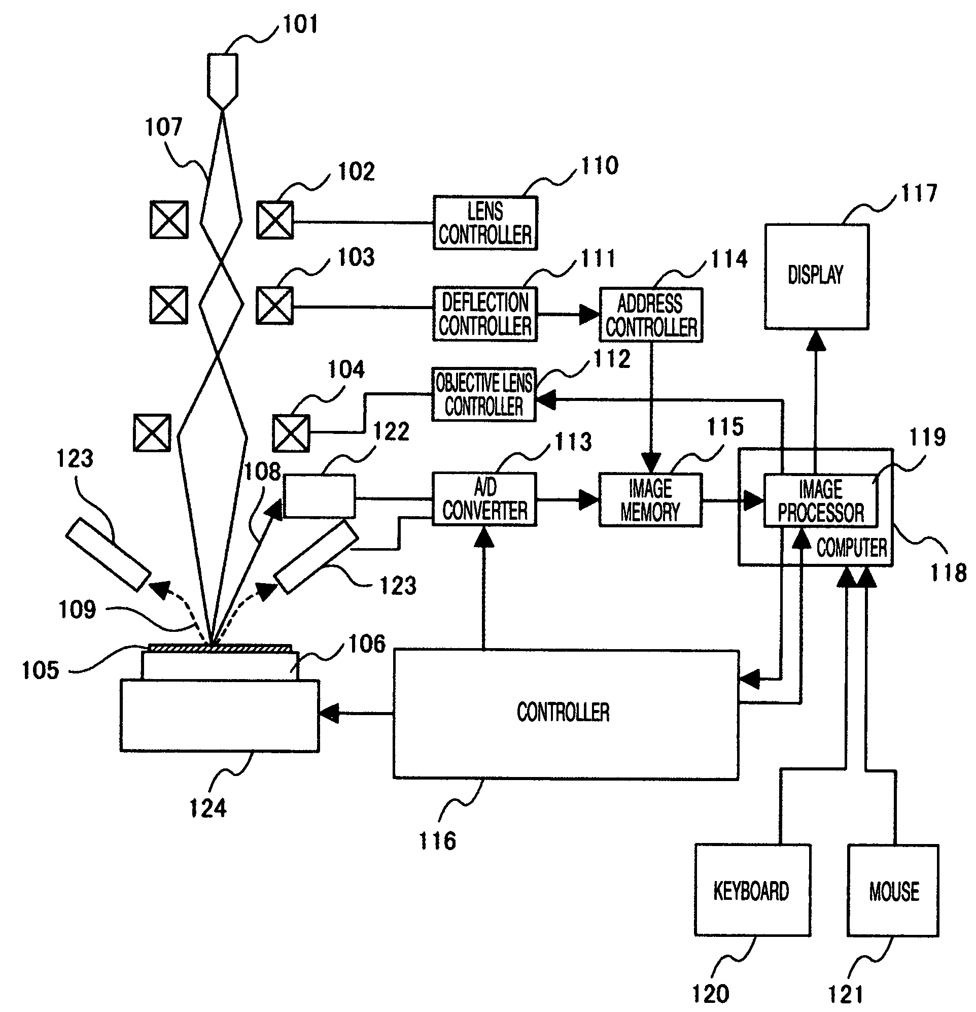
Scanning electron microscope
a scanning electron microscope and microscope technology, applied in the field of scanning electron microscopes, can solve the problems of inability to cope with the autofocus adjustment function, low level of raised and recessed portions on the surface, and various kinds of foreign matter or defects causing the operation of the faulty device, etc., to achieve stable autofocus adjustment, stable autofocus adjustment, and stable autofocus adjustment
- Summary
- Abstract
- Description
- Claims
- Application Information
AI Technical Summary
Benefits of technology
Problems solved by technology
Method used
Image

Examples
embodiment 1
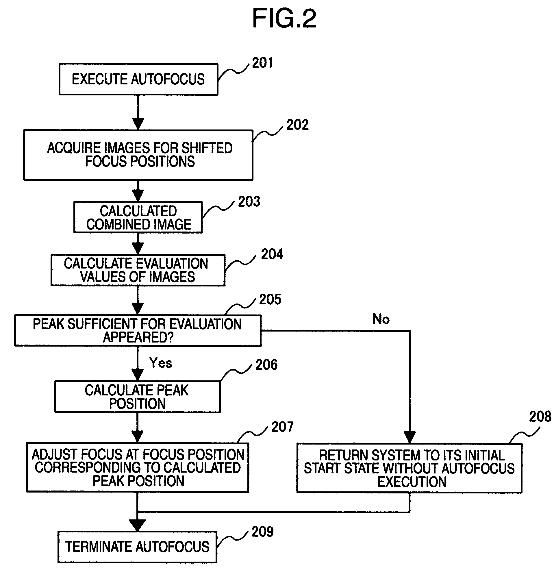
[0035]FIG. 2 is a flow chart showing a focus adjusting procedure. In FIG. 2, with such an arrangement as mentioned above, focus adjustment is executed according to a procedure of steps 201 to 209. In the step 202, first of all, images by each detector are picked up at focus positions stepwise shifted by the objective lens controller 112. In this step, a set of images with focus states gradually varying with focus movement can be obtained.
[0036]In the step 203, next, the set of images are combined. The images acquired in the step 202 are calculated according to a previously-registered equation by the image processor 119.
[0037]FIG. 3 shows a diagram for explaining the processing contents of the step 203. Images are picked up with varying focuses for each detector in the step 202. Groups of images 301, 302, and 303 are images obtained from the detectors of secondary electron, reflected electron (L), and reflected electron (R) respectively. In this connection, the reflected electron (L)...
embodiment 2
[0046]FIG. 7 shows a flow chart of the embodiment 2. The embodiment 2 shows an example which includes the contents of the embodiment 1 and wherein calculation contents can be set by a user. The embodiment 2 is different from the embodiment 1 only in the operation of a step 701 shown in FIG. 7, that is, in that the user sets the calculation contents immediately before the system performs the autofocus adjustment so as to calculate a combined image on the basis of the set calculation contents. The calculation contents can be specified by the user in the form of such contents displayed by a GUI as shown in FIG. 6.
[0047]A display screen 601 shown in FIG. 6 is the GUI for setting a coefficient (i.e., image addition ratio) to each detector in the aforementioned equation (1). On the GUI, the user can uniquely set a mixture ratio of respective images in the equation (1) to enhance a focus accuracy according to each image. In this example, the user can set the above ratio by adjusting slide ...
embodiment 3
[0049]FIG. 8 shows a flow chart of this embodiment 3. The drawing is substantially the same as the embodiment 2, but different therefrom in an image combining system and a parameter selecting method. The difference from the embodiment 2 is a function of automatically setting detectors for acquiring images. FIG. 9 is a diagram for explaining parameters used in a calculation method selecting process in the embodiment 3.
[0050]When the user selects the automatic detector selection setting button 609 in FIG. 6, this causes such sets of parameters 903, 904 and 905 as shown by a functional diagram 901 in FIG. 9 to be stored in the computer 118 each time that the autofocusing operation is executed. A step 810 is provided to determine an equation and parameters prior to the image calculation as shown by a functional diagram 902 in FIG. 9. In the determining method, one of the equations having the highest frequency of execution and parameters are set on the basis of history data previously st...
PUM
 Abstract
Description
Claims
Application Information
 - R&D
- Intellectual Property
- Life Sciences
- Materials
- Tech Scout
- Unparalleled Data Quality
- Higher Quality Content
- 60% Fewer Hallucinations
Browse by: Latest US Patents, China's latest patents, Technical Efficacy Thesaurus, Application Domain, Technology Topic, Popular Technical Reports.
© 2025 PatSnap. All rights reserved.Legal|Privacy policy|Modern Slavery Act Transparency Statement|Sitemap|About US| Contact US: help@patsnap.com