Liquid crystal display device and method of manufacturing the same

a display device and liquid crystal technology, applied in non-linear optics, instruments, optics, etc., can solve the problems of degrading the display quality of the lcd, difficult to obtain the storage capacitance cst in the lcd, and the miniaturization and portability of the lcd display device, so as to reduce the number of mask processes, reduce the defect of light leakage, and achieve the effect of sufficient obtaining storage capacitan

Inactive Publication Date: 2010-05-18
LG DISPLAY CO LTD
View PDF8 Cites 4 Cited by
  • Summary
  • Abstract
  • Description
  • Claims
  • Application Information

AI Technical Summary

Benefits of technology

[0036]An advantage of the present invention is to provide an LCD and a method of manufacturing the same for reducing the number of mask processes and sufficiently obtaining a storage capacitance.
[0037]Another advantage of the present invention is to provide an LCD and a method of manufacturing the same for reducing the number mask processes so that the step difference of the electrodes may be minimized in order to reduce a light leakage defect.

Problems solved by technology

However, the CRT display device also has disadvantages in miniaturization and portability.
The number of mask processes directly relates to the manufacturing cost of the LCD.
However, it is very difficult to obtain the storage capacitance Cst in the LCD shown in FIG. 1 because the gate insulating layer 2 and the passivation layer 9 are formed between the first storage electrode 17b and the second storage electrode 15.
If the storage capacitance Cst is not sufficiently obtained, as in the related art, display quality of the LCD is degraded.

Method used


Image

  • Liquid crystal display device and method of manufacturing the same
  • Liquid crystal display device and method of manufacturing the same
  • Liquid crystal display device and method of manufacturing the same

Examples


Embodiment Construction

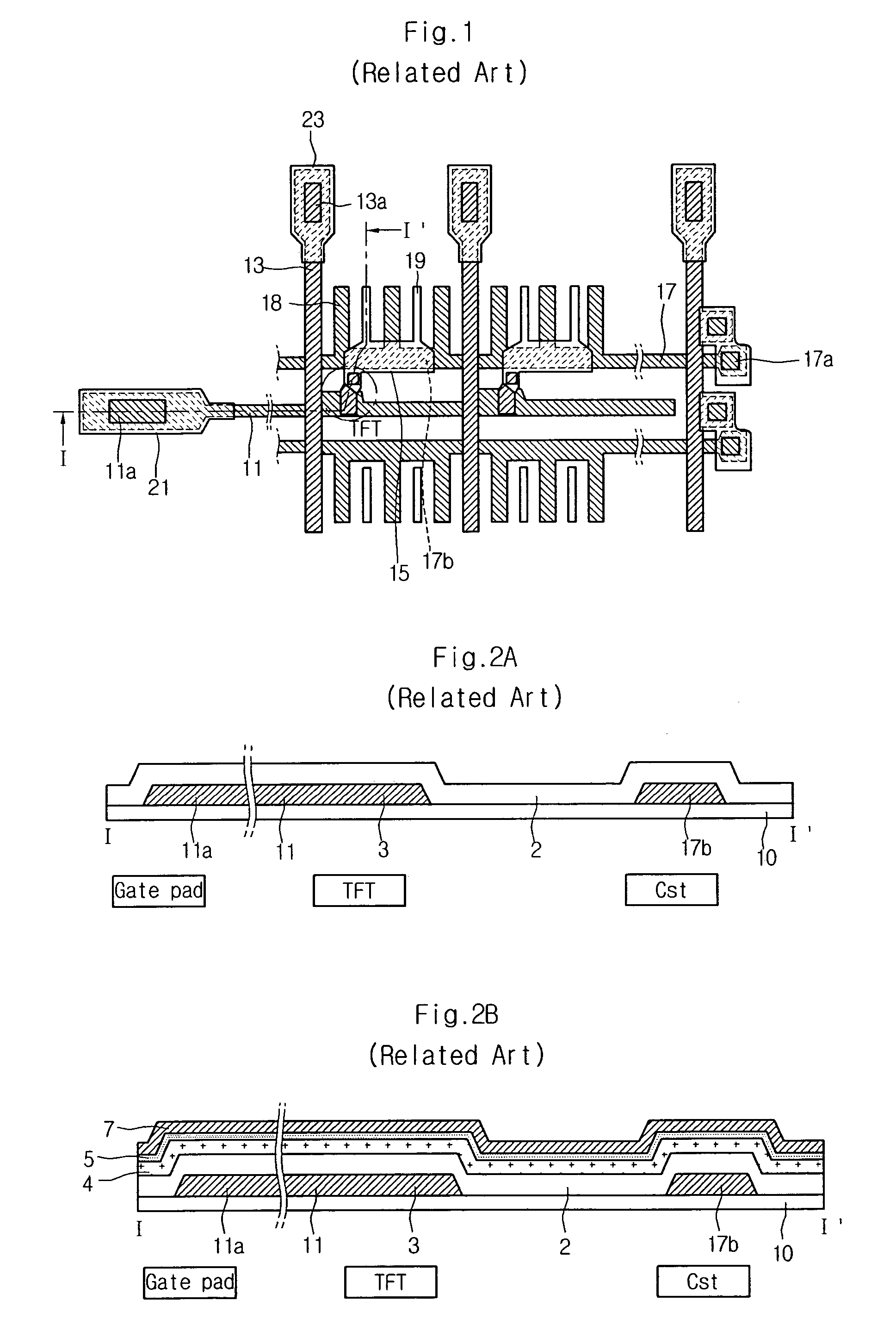
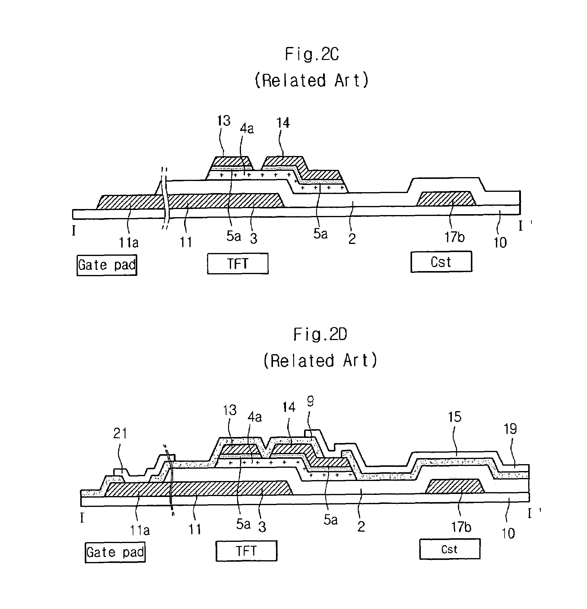
[0056]Reference will now be made in detail to embodiments of the present invention, examples of which are illustrated in the accompanying drawings. Wherever possible, the same reference designations will be used throughout the drawings to refer to the same or similar parts.

[0057]FIG. 3 is a plan view of an IPS mode LCD according to an embodiment of the present invention.

[0058]As shown in FIG. 3, a unit pixel region is defined by a gate line 111 and a data line which are arranged to cross each other. The gate line 111 receives a driving signal, and the data line includes a first data line 113 and a second data line 123 for receiving a data signal. The first data line 113 and the second data line 123 may overlap with each other.

[0059]The first data line 113 is an opaque metal and is formed when a channel layer is formed along a halftone pattern. The second data line 123 is a line patterned to overlap along the first data line 113 when a pixel electrode 119 is formed by depositing a tr...


PUM

PropertyMeasurementUnit
transparentaaaaaaaaaa
storage capacitanceaaaaaaaaaa
brightnessaaaaaaaaaa

Abstract

An LCD include a gate line, a first data line and a second data line arranged to cross each other, thereby defining a unit pixel region, a TFT disposed at a region where the gate line, the first data line and the second data line cross, and having a passivation layer on an exposed channel layer, a common line disposed in parallel to the gate line, a first storage electrode integrally formed with the common line for forming a storage capacitance in the unit pixel region, a second electrode disposed to overlap with the first storage electrode, common electrodes branched from the first storage electrode and disposed at the unit pixel region, and pixel electrodes branched from the second storage electrode and alternately disposed with the common electrodes.

Description

[0001]This application claims the benefit of Korean Patent Application No. 10-2004-0116346 filed on Dec. 30, 2004, which is hereby incorporated by reference for all purposes as if fully set forth herein.BACKGROUND OF THE INVENTION[0002]1. Field of the Invention[0003]The present invention relates to a liquid crystal display device and a method of manufacturing the same, and more particularly, to a liquid crystal display device and a method of manufacturing the same, capable of reducing processes required to manufacture an LCD and capable of obtaining a storage capacitance, thereby providing an improved display quality.[0004]2. Description of the Related Art[0005]A liquid crystal display module is gaining importance as an information display device. A cathode ray tube (CRT) has advantages in performance and has been widely used until now. However, the CRT display device also has disadvantages in miniaturization and portability.[0006]In order to overcome such disadvantages of the CRT, ...

Claims


Application Information

Patent Timeline
Patent Type & Authority Patents(United States)
IPC IPC(8): G02F1/1343
CPCG02F1/134363G02F2001/136236G02F2001/136231G02F1/136213G02F1/136231G02F1/136236G02F1/136
Inventor LIM, BYOUNG HO
Owner LG DISPLAY CO LTD
Why Eureka
Try Eureka