Chip antenna, an antenna device, and a communication equipment
a technology of antenna device and antenna, applied in the direction of resonant antenna, substantially flat resonant elements, protective material radiating elements, etc., can solve the problems of narrow bandwidth, difficult application to use, restricted mounting space for electronic parts in communication equipment, especially in portable communication equipment, etc., to achieve excellent shock resistance, wide bandwidth, and efficient mounting within communication equipment
- Summary
- Abstract
- Description
- Claims
- Application Information
AI Technical Summary
Benefits of technology
Problems solved by technology
Method used
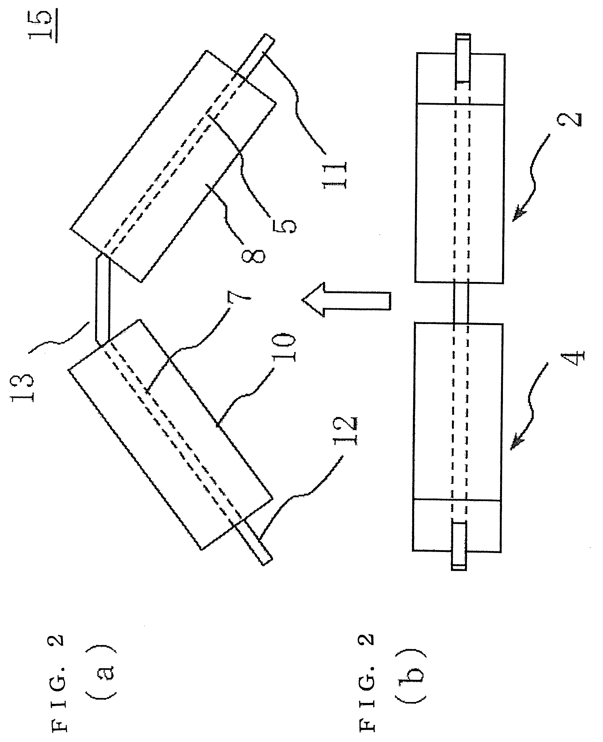
Image


Examples
example
[0121]In production of the magnetic base in this example, Fe2O3, BaO (BaCO3 is used), and CoO (Co3O4 is used), these are the principal component, were first mixed with 60 mol %, 20 mol %, and 20 mol, respectively. CuO of the composition shown in Table 1 to this principal component 100 weight part was added, and it was mixed with the wet ball mill by using water for 16 hours (No 1-7).
[0122]Next, temporary sintering was carried out at 1000˜C in atmosphere in 2 hours after drying such mixed powder. Such temporary sintering powder was ground by the wet ball mill by using water for 18 hours. Binder (PVA) 1% was added to the obtained pulverized powder, and granulated. After granulation, compression molding was carried out to ring shape and rectangular parallelepiped shape. Then, sintering was carried out at 1200° C. in oxygen environment for 3 hours. The density, initial magnetic permeability μ at 25° C., and loss factor tan δ, in the ring shape ceramics with the outer diameter of 7.0 mm,...
PUM
 Abstract
Description
Claims
Application Information
 - R&D
- Intellectual Property
- Life Sciences
- Materials
- Tech Scout
- Unparalleled Data Quality
- Higher Quality Content
- 60% Fewer Hallucinations
Browse by: Latest US Patents, China's latest patents, Technical Efficacy Thesaurus, Application Domain, Technology Topic, Popular Technical Reports.
© 2025 PatSnap. All rights reserved.Legal|Privacy policy|Modern Slavery Act Transparency Statement|Sitemap|About US| Contact US: help@patsnap.com