
Working shape prediction method, working requirement determination method, working method, working system, method of manufacturing semiconductor device, computer program, and computer program storage medium

a technology of working shape and working requirement, applied in semiconductor/solid-state device testing/measurement, manufacturing tools, lapping machines, etc., can solve the problems of wiring interruption and drop in electrical capacitance, individual processes involved in semiconductor manufacturing processes have become more numerous and complicated, and achieve the effect of quickly determining working conditions

Active Publication Date: 2010-03-30
NIKON CORP
View PDF12 Cites 5 Cited by
  • Summary
  • Abstract
  • Description
  • Claims
  • Application Information

AI Technical Summary

Benefits of technology

The present invention provides a method for predicting the shape of a worked object in a working apparatus, such as a polishing apparatus, by breaking down the worked shape into elements and determining the relationship between these elements and the working conditions that caused them. This allows for accurate prediction of the worked shape, even when the working conditions are complicated. The method is simple and accurate, and can be used in various manufacturing processes. The invention also provides a computer program for implementing the method and a computer program storage medium for storing the method.

Problems solved by technology

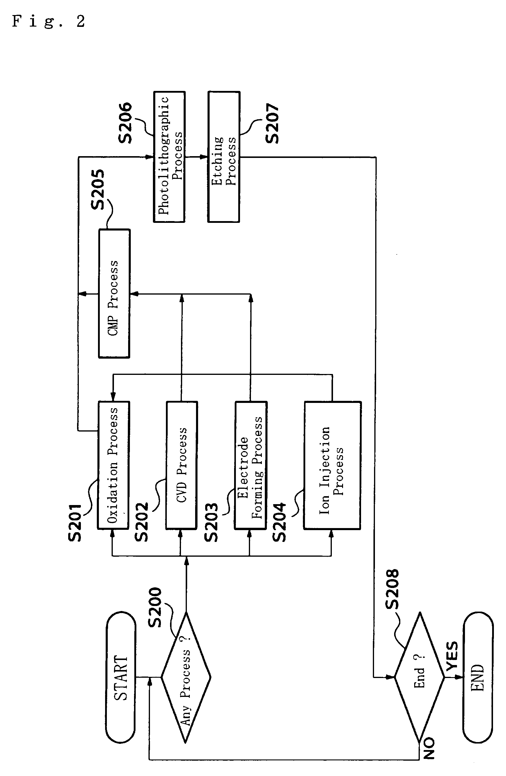
As semiconductor integrated circuits have become finer and more highly integrated, the individual processes involved in semiconductor manufacturing processes have become more numerous and complicated.
As a result, the surfaces of semiconductor devices are not always flat.
The presence of step differences on the surfaces of semiconductor devices leads to step breakage of wiring and local increases in resistance, etc., and thus causes wiring interruptions and drops in electrical capacitance.
In insulating films, furthermore, such step differences also lead to a deterioration in the withstand voltage and the occurrence of leaks.
As a result, the focal depth of the projection lenses used in such semiconductor exposure apparatuses has become substantially shallower.
Accordingly, such a method involves the trouble of setting the polishing conditions anew for each polishing operation.
Numerous wafers are used in this test polishing, and considerable time is required in order to determine the polishing conditions.
However, even if such fine adjustments are thus made for each production lot, a problem remains in that variation within lots cannot be handled.
In conventional polishing apparatuses in which the polishing body is larger than the wafer being polished, the following problem arises: namely, the size of the apparatus itself increases as the diameter of the wafer increases.
Another drawback is that the replacement of consumed parts that require replacement, such as the polishing pad, is extremely difficult because of its large size.
Moreover, in cases where there are indentations and projections in the surface of the wafer prior to polishing due to irregularities in film formation, it is extremely difficult to polish the surface to a flat surface by the appropriate treatment of such indentations and projections.
In the case of conventional polishing apparatuses, it is difficult to meet such demands.
Specifically, the number of polishing conditions is increased, and at the same time, the polishing conditions become more complicated; furthermore, the frequency with which the polishing conditions must be determined is increased, and more wafers and time are required for the determination of a single polishing condition.
Moreover, even in cases where fine adjustments are not required, since the polishing body is small, the polishing conditions are still complicated compared to those in a conventional polishing apparatus using a large polishing body.
Accordingly, as a result of the addition of such control actions, the complexity of the polishing conditions is greatly increased.
However, in the polishing process, the polishing body undergoes elastic deformation, and the flow of the polishing agent between the polishing body and the object of polishing is complicated; furthermore, frictional heat is generated during polishing.
As a result, it is difficult to express the overall polishing process in terms of numerical equations, so that a numerical model with general applicability has not yet been obtained.

Method used


Image

  • Working shape prediction method, working requirement determination method, working method, working system, method of manufacturing semiconductor device, computer program, and computer program storage medium
  • Working shape prediction method, working requirement determination method, working method, working system, method of manufacturing semiconductor device, computer program, and computer program storage medium
  • Working shape prediction method, working requirement determination method, working method, working system, method of manufacturing semiconductor device, computer program, and computer program storage medium

Examples


embodiment 1

(Embodiment 1)

[0107]The polishing of a wafer with a diameter of 200 mm which had a Cu pattern inside was performed using a polishing apparatus in which the polishing pad was smaller than the wafer. This polishing was performed using an annular polishing pad with an external diameter of 150 mm and an internal diameter of 50 mm under the following conditions: head rpm 400 rpm, wafer rpm 200 rpm, polishing time 60 sec, slurry 100 ml (RD98052, FUJIMI Incorporated). The wafer had a film thickness of 1.5 μm, and the initial film thickness was extremely uniform.

[0108]Six wafers were polished under different polishing conditions determined by combinations of the swinging conditions (polishing starting position, amount of swinging), and six relationships between the polishing conditions constituting elements and the worked shape were determined. The polishing time was 60 seconds in all six sets of conditions. The relationships between the swinging conditions and the worked shapes (amounts of...

embodiment 2

(Embodiment 2)

[0114]Combinations of four of the conditions selected as conditions in Embodiment 1 were converted into a single swinging pattern from the probability of the presence of the center of the polishing pad. FIG. 10 shows the results obtained. In FIG. 10, the horizontal axis indicates the center coordinates of the head (corresponding to the wafer position), and the vertical axis indicates the swinging velocity. The triangles indicate the calculated values, and indicate swinging at the corresponding swinging velocity at the specified head center coordinates. The pattern shown in FIG. 10 indicates swinging at a swinging velocity of 364 mm / min when the head center coordinates are between 23 mm and 38 mm, swinging at a swinging velocity of 1092 mm / min when the head center coordinates are between 38 mm and 53 mm, and swinging at a swinging velocity of 401 mm / min when the head center coordinates are between 53 mm and 68 mm.

[0115]When polishing was performed under these conditions...

embodiment 3

(Embodiment 3)

[0116]The polishing of a wafer with a diameter of 200 mm in which a Cu pattern was formed inside was performed using a polishing apparatus in which the polishing pad was smaller than the wafer. Cu wafers from a different wafer lot from that used in Embodiment 1 were used in the polishing of this embodiment. The wafer of this lot had a protruding shape in which the film thickness of the wafer was 1.6 μm in the central portion of the wafer, and 1.45 μm in the edge portions of the wafer.

[0117]For the wafers having this protruding film thickness distribution, the target residual film thickness was set at 0.9 μm, and conditions for realizing a flat worked shape were determined using combinations of the six sets of polishing conditions constituting elements used in Embodiment 1. The simulation method was the same as that used in Embodiment 1. As a result, it was found that polishing for 24 seconds under condition 1, 6 seconds under condition 3 and 30 seconds under condition ...


PUM


Abstract

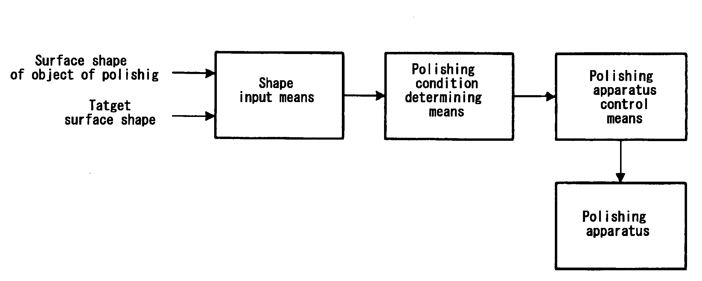
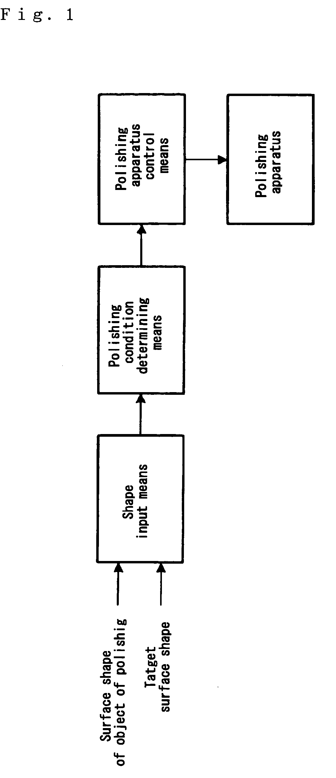
The relationship between polishing conditions constituting elements and the worked shape (amount of polishing) obtained by way of these polishing conditions is input beforehand into polishing condition determining mechanism along with the type of the object of polishing, and polishing conditions (invariable polishing conditions) that are used in common for the polishing of this object of polishing. The polishing condition determining mechanism determines the polishing conditions on the basis of these conditions. Specifically, the above-mentioned polishing conditions constituting elements are given in a time series, or combinations of the above-mentioned polishing conditions constituting elements are converted into variations in the swinging velocity of the polishing body, and the swinging velocity corresponding to the swinging position is determined. The polishing apparatus control mechanism input the polishing conditions determined by the polishing condition determining mechanism, and control the polishing apparatus so that these polishing conditions are realized. As a result, working conditions for obtaining a specified worked shape in a working apparatus can be simply and accurately determined.

Description

TECHNICAL FIELD[0001]The present invention relates to a method for predicting the worked shape that is obtained in cases where an object of working is worked, a method for determining the working conditions under which this object of working is worked, a working method for working this object of working, a working system for working this object of working, a semiconductor device manufacturing method using this working method and working system, a computer program which performs the method for determining working conditions, and a computer program storage medium on which this computer program is stored. Furthermore, the term “working” used in the present specification and claims refers to mechanical working such as polishing and grinding.BACKGROUND TECHNOLOGY[0002]As semiconductor integrated circuits have become finer and more highly integrated, the individual processes involved in semiconductor manufacturing processes have become more numerous and complicated. As a result, the surfa...

Claims


Application Information

Patent Timeline
Patent Type & Authority Patents(United States)
IPC IPC(8): B24B49/00B24B51/00B24B37/04H01L21/304H01L21/321
CPCB24B37/042B24B49/00H01L22/26B24B49/04H01L21/3212H01L21/304
Inventor SENGA, TATSUYAISHIKAWA, AKIRAUEDA, TAKEHIKO
Owner NIKON CORP
Learn More