
Circuit design optimization of integrated circuit based clock gated memory elements

a technology of memory elements and integrated circuits, applied in computer aided design, program control, instruments, etc., can solve the problems of insufficient comparison of inputs, current synthesis tools generally do not allow changing the number of memory elements, and the power consumed by modern ics continues to escalate, so as to simplify the logic of the integrated circuit

Active Publication Date: 2010-03-09
SIEMENS PROD LIFECYCLE MANAGEMENT SOFTWARE INC
View PDF8 Cites 10 Cited by
  • Summary
  • Abstract
  • Description
  • Claims
  • Application Information

AI Technical Summary

Benefits of technology

The present invention provides a solution for identifying and eliminating redundant clock gated circuits in a digital design, which can save energy and improve the efficiency of the design. The invention analyzes all clock gated circuits and generates a canonical representation of the inputs and outputs of each circuit. This representation is then compared with other circuits to identify duplicate circuits, which can then be eliminated. The invention also provides a method for logic simplification of clock gated circuits, which can result in potential savings in fabrication costs and reduced energy usage. The invention can be used at an early stage in the design cycle and can be implemented using software or hardware tools. Overall, the invention improves the design of integrated circuits with clock gated circuits.

Problems solved by technology

Due to the increased density of modern integrated circuits (ICs), the amount of power consumed by modern ICs continues to escalate.
Current synthesis tools generally do not allow changing the number of memory elements used to implement a design.
Under clock gating, however, it does not suffice to compare the inputs.

Method used


Image

  • Circuit design optimization of integrated circuit based clock gated memory elements
  • Circuit design optimization of integrated circuit based clock gated memory elements
  • Circuit design optimization of integrated circuit based clock gated memory elements

Examples


Embodiment Construction

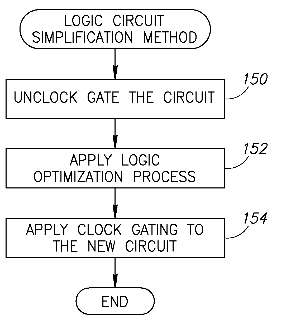
[0040]The present invention is a method to optimize the design of integrated circuits containing clock gated circuits by identifying functionally equivalent clock gated circuits in canonical representations thereof and simplifying the logic in the clock gated circuits. Identification of functionally equivalent clock gated circuits enables the deletion of duplicate memory elements from the design, while logic simplification redesigns the circuit with the goal of reducing combinational logic while retaining the same logical function.

[0041]The invention enables synthesis tools to be developed which generate more efficient digital designs containing clock gated circuits. Both the elimination of duplicate memory elements and the logical simplification of combinational logic result in more energy efficient digital designs.

[0042]Canonical representations allow mathematical objects to be uniquely identified by indicating a particular representation from a variety of representations. For exa...


PUM


Abstract

A novel method for optimizing the design of digital circuits containing clock gated memory elements. The method unclock gates memory elements by adding necessary feedback loops. Logic functions of memory element outputs in the circuit are viewed as a whole, rather than as separate functions for each input. Detection of duplicate unclock gated memory elements is then effected by identifying identical canonical representations of said unclock gated memory elements. Identified duplicate clock gated memory elements can then be eliminated from the original digital circuit. Further optimization can be accomplished by applying standard logic optimization algorithms to all unclock gated memory elements in said digital circuit. The resulting optimized circuit is clock gated and replaces the original clock gated circuit in said digital circuit.

Description

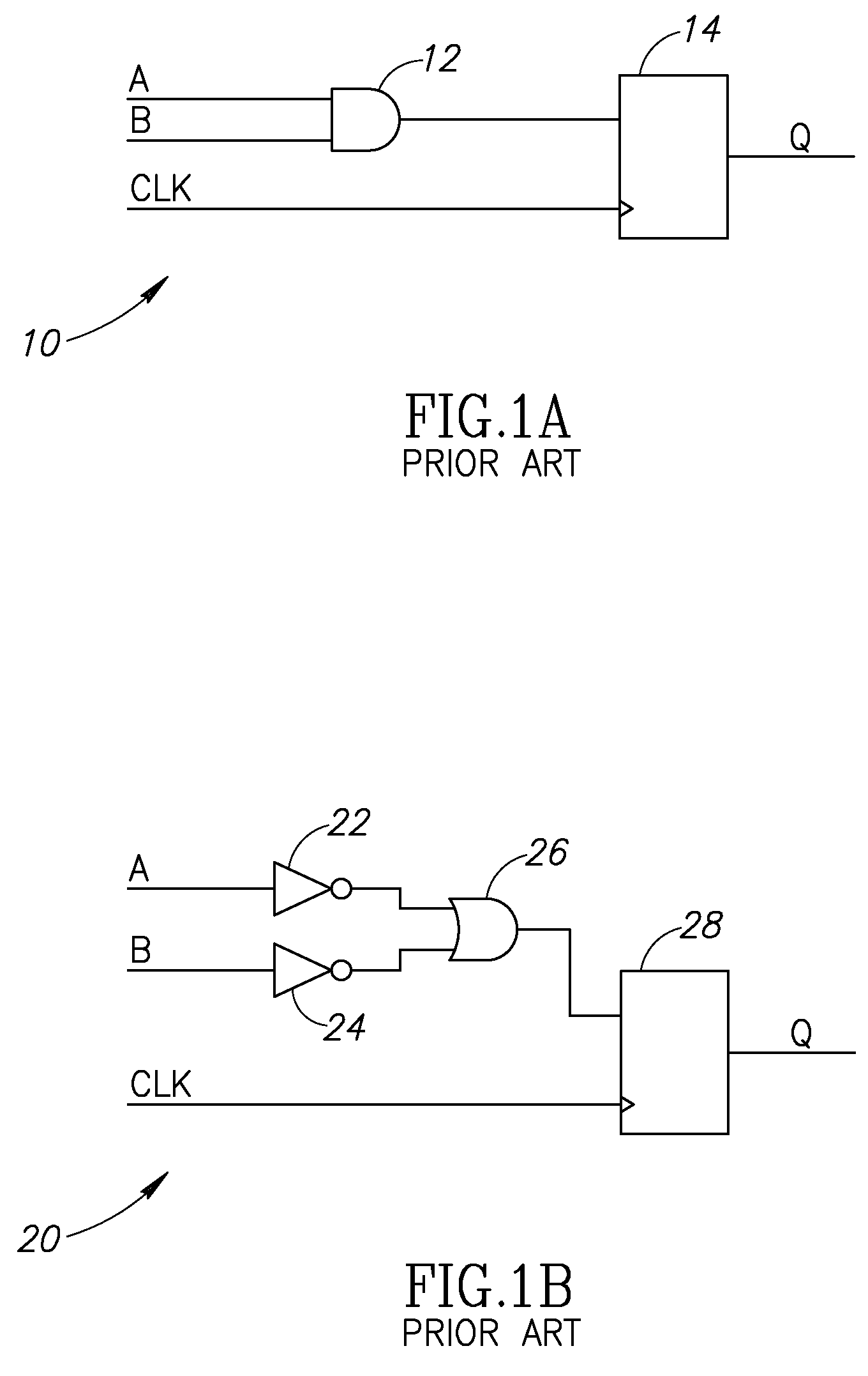
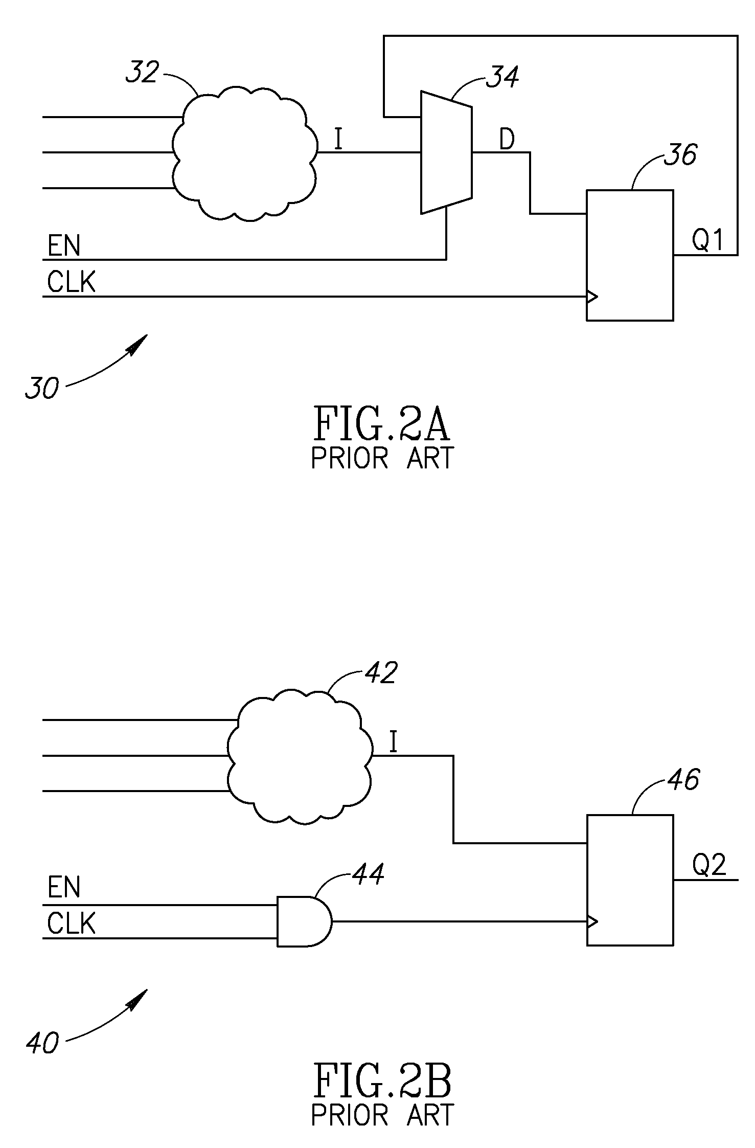
FIELD OF THE INVENTION[0001]The present invention relates to the field of integrated circuit design tools and more particularly relates to a method of optimizing logic design by eliminating duplicate memory elements and simplifying logic circuits for integrated circuit designs where memory elements are toggled by an enable pin or a clock gate.BACKGROUND OF THE INVENTION[0002]Logic synthesis is well known in the integrated circuit design arts. Logic synthesis is the process of transforming a register-transfer level (RTL) description of a circuit into an implementation consisting of a set of interconnected gates. During this process logically equivalent memory elements can be implemented using different design elements in order to meet necessary constraints.[0003]An example prior art original circuit design is shown in FIG. 1A. The circuit, generally referenced 10, comprises AND gate 12 and a memory element 14 which may comprise a latch, register, flip-flop, etc. The circuit directly ...

Claims


Application Information

Patent Timeline
Patent Type & Authority Patents(United States)
IPC IPC(8): G06F17/50
CPCG06F17/505G06F2217/62G06F30/396G06F30/327G06F2117/04
Inventor ARBEL, ELIEISNER, CYNTHIA RAEITSKOVICH, ALEXANDERMAEDING, NICOLAS
Owner SIEMENS PROD LIFECYCLE MANAGEMENT SOFTWARE INC
Learn More