Apparatus for pattern replication with intermediate stamp
a technology of pattern replication and intermediate stamp, which is applied in the direction of dough shaping, manufacturing tools, food shaping, etc., can solve the problems of reducing replication fidelity, destroying the imprint process, and the imprint process described above exhibits some difficulties, so as to minimize wear and damage. risk
- Summary
- Abstract
- Description
- Claims
- Application Information
AI Technical Summary
Benefits of technology
Problems solved by technology
Method used
Image
Examples
example 1
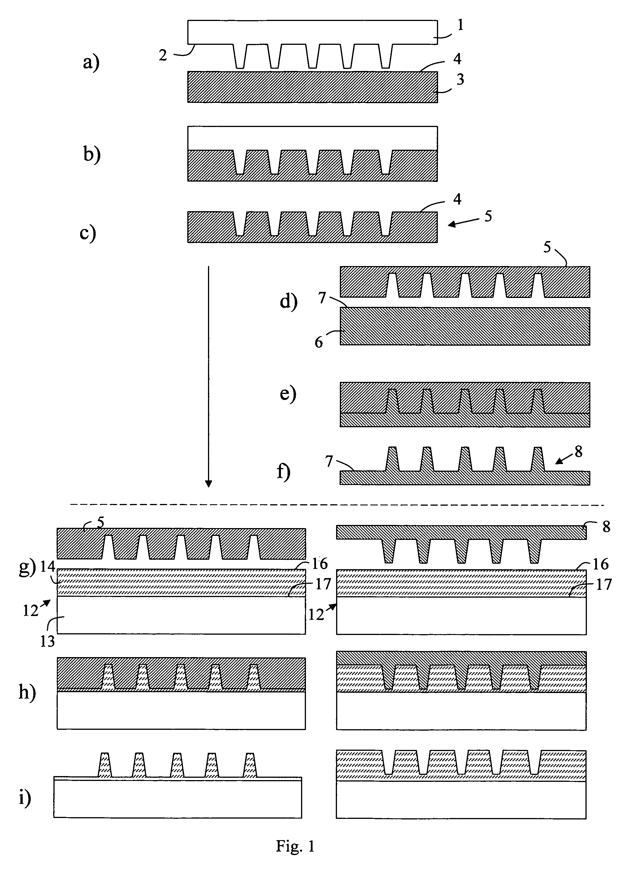
[0136]A nickel template whose surface exhibits a line pattern, having a line width of 80 nm and a height of 90 nm has been imprinted into a Zeonor ZF14 foil at 150° C. and 50 bar for 3 min. None of the surfaces have been treated by any additional coating such as, e.g. anti-adhesion layers. The release temperature was 135° C., at which the Zeonor foil could mechanically be removed from the nickel surface without damaging the pattern of neither the template nor the replica. The Zeonor foil has been used as a new template, which has been imprinted into a 100 nm thick SU8 film. The SU8 film was spin-coated onto a 20 nm LOR film, previously spin-coated onto a silicon substrate. Also here, none of the surfaces has been treated by an additional coating, having the purpose to improve the anti-adhesion behavior between the SU8 film and the Zeonor foil. The imprint was performed at 70° C. and 50 bar for 3 min. The SU8 film was exposed to UV-light for 4 seconds through the optically transparen...
example 2
[0137]A nickel template whose surface exhibits a BluRay pattern having structure heights of 100 nm and widths of 150 nm—investigated by AFM—has been imprinted into a Zeonor ZF14 using the same process and the same parameters as already described in Example 1. The Zeonor foil has been used as a new template, which has been imprinted into a 100 nm thick SU8 film. Also here the same process and the same parameters as already described in Example 1 have been used. The AFM image of an imprint result in the SU8 film deposited on a silicon wafer is shown in FIG. 3.
example 3
[0138]A nickel template has been used whose surface contains micro-meter patterns with high aspect-ratios ranging from 1-28. The feature size ranges from 600 nm to 12 μm, at a height of 17 μm. The surface has been covered by a phosphate-based anti-adhesion film before the imprint. The nickel template has been imprinted into a polycarbonate foil at 190° C. and 50 bar for 3 min. The surface of the polycarbonate foil has not been treated by an additional coating, having the purpose to improve the anti-adhesion behavior between the Ni template and the polycarbonate film. The release temperature was 130° C., at which the polycarbonate foil could mechanically be removed from the nickel surface without damaging the pattern of neither the template nor the replica. The polycarbonate foil has been used as a new template for an imprint into a Topas foil. The imprint has been performed at 120° C. and 50 bar for 3 min. None of the surfaces has been disposed by an additional coating, having the p...
PUM
| Property | Measurement | Unit |
|---|---|---|
| pressure | aaaaa | aaaaa |
| flow time | aaaaa | aaaaa |
| height | aaaaa | aaaaa |
Abstract
Description
Claims
Application Information
 - R&D
- Intellectual Property
- Life Sciences
- Materials
- Tech Scout
- Unparalleled Data Quality
- Higher Quality Content
- 60% Fewer Hallucinations
Browse by: Latest US Patents, China's latest patents, Technical Efficacy Thesaurus, Application Domain, Technology Topic, Popular Technical Reports.
© 2025 PatSnap. All rights reserved.Legal|Privacy policy|Modern Slavery Act Transparency Statement|Sitemap|About US| Contact US: help@patsnap.com


