
Wire bond encapsulant application control

a technology of encapsulant and wire bonding, which is applied in the direction of semiconductor devices, semiconductor/solid-state device details, printing, etc., can solve the problems of encapsulant bead not being straight, encapsulant volume and placement on the die are not very accurate, and the encapsulant can hamper the wiping conta

Inactive Publication Date: 2010-02-09
MEMJET TECH LTD +1
View PDF24 Cites 8 Cited by
  • Summary
  • Abstract
  • Description
  • Claims
  • Application Information

AI Technical Summary

Benefits of technology

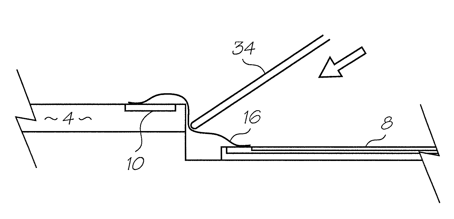
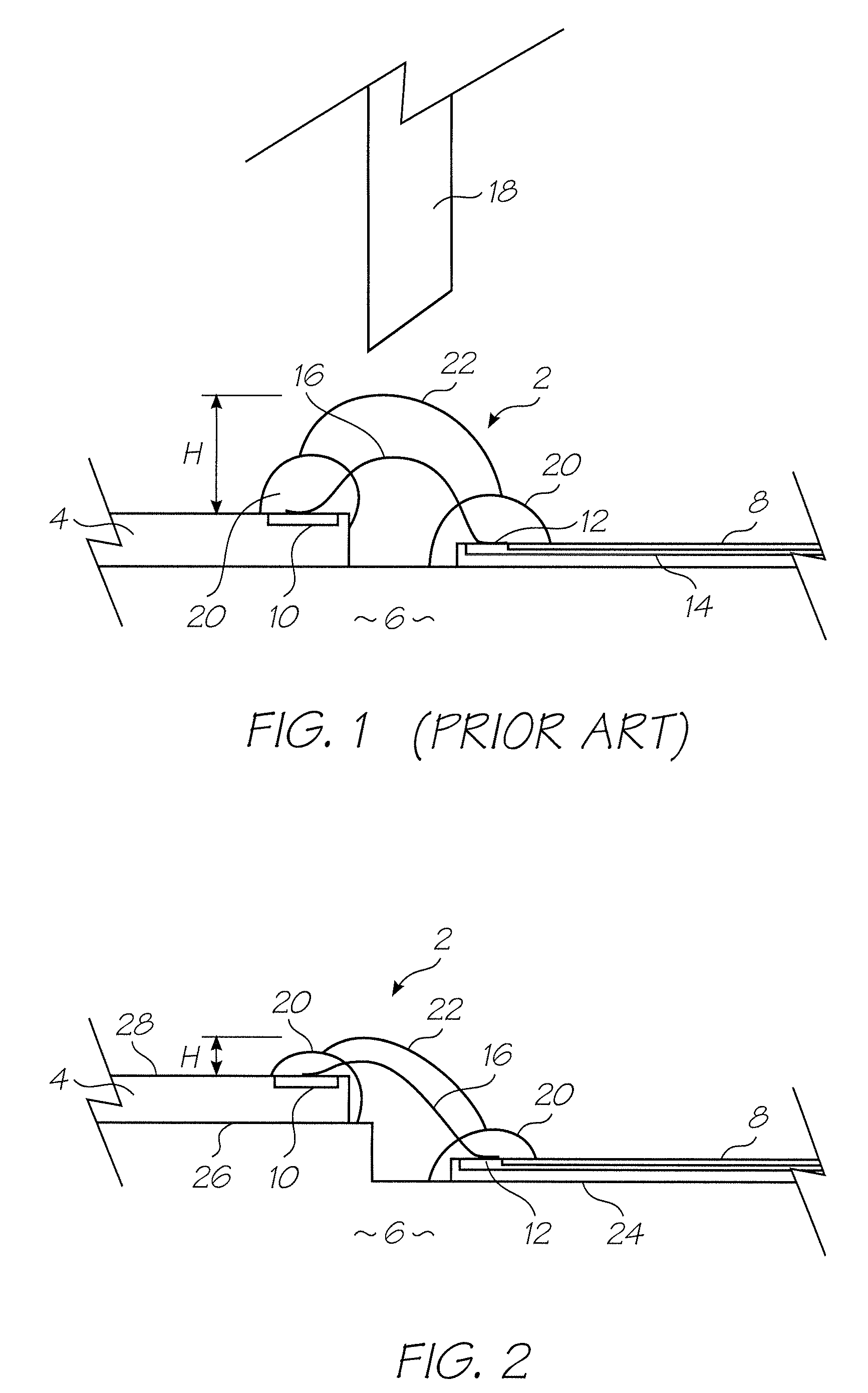
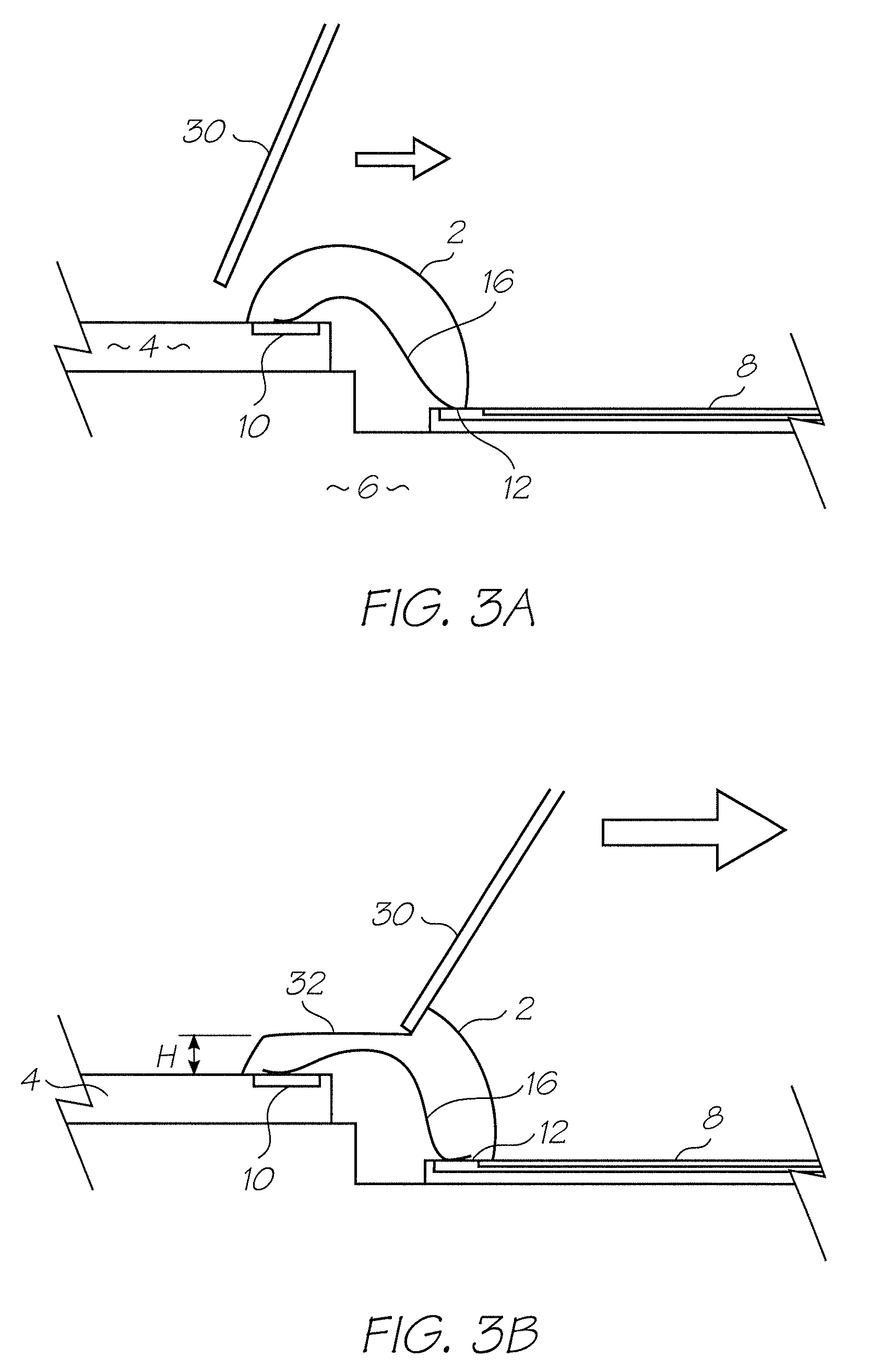
The present invention provides a microprocessor device with a raised chip mounting area and a conductor mounting area, where a chip is supported on the chip mounting area and a flexible printed circuit board with conductive pads is supported on the conductor mounting area. The chip mounting area is raised relative to the conductor mounting area, which allows the top of the chip to be closer to the active surface of the chip. This reduces the profile of the encapsulant bead, which is important for the function of the chip. The wire bonds connecting the chip to the flexible printed circuit board are plastically deformed, and a bead of encapsulant is applied over the wire bonds to further reduce the profile of the bead. The method also includes steps of pushing on the wire bond to collapse the arc and plastically deform the wire bond, and releasing the wire bonds to maintain the wire bond in a flatter profile shape. The strength of the wire bond is relatively small, but the method allows for a robust wire bond that can withstand a certain degree of work hardening. The method also includes steps of applying a bead of encapsulant over the wire bond and moving a profiling surface over the active surface to flatten the bead of encapsulant. The invention provides a microprocessor device with improved wire bond reliability and a flattened encapsulant bead profile.

Problems solved by technology

Similarly, if a cleaning surface is wiped across the nozzles, the bead of encapsulant can hamper the wiping contact.
Another problems arises because of sides of the encapsulant bead are not straight.
The encapsulant volume and placement on the die is not very accurate.
Variations in the pressure from the pump or slight non-uniformities in the speed of the needle cause the side of the bead contacting the active surface to be reasonably crooked.

Method used


Image

  • Wire bond encapsulant application control
  • Wire bond encapsulant application control
  • Wire bond encapsulant application control

Examples


Embodiment Construction

[0121]FIG. 1 shows a common technique used for applying a bead encapsulant to wire bonds. A die 4 is mounted to a supporting structure 6 adjacent the edge of a flex PCB 8 (flexible printed circuit board). The die 4 has a line of contact pads 10 along one edge and the flex PCB 8 has corresponding bond pads 12. Wire bonds 16 extend from the bond pads 10 to the bonds pads 12. Power and data is transmitted to the die 4 via conductive traces 14 in the flex PCB 8. This is a simplified representation of the dies mounted within many electronic devices. The printhead IC dies mounted to the LCP (liquid crystal polymer) molding to receive print data from an adjacent flex PCB, as described in U.S. Ser No. 11 / 014769 (Our Docket RRC001US) incorporated herein by cross reference, is one example of this type of die mounting arrangement. The ordinary worker will appreciate that the die may also be mounted directly to a hard PCB with traces formed thereon.

[0122]The wire bonds 16 are covered in a bead ...


PUM


Abstract

A method of applying encapsulant to a die mounted to a support structure by providing a die mounted to the support structure, the die having a back surface in contact with the support structure and an active surface opposing the back surface, the active surface having electrical contact pads, positioning a barrier proximate the electrical contact pads and spaced from the active surface to define a gap and, depositing a bead of encapsulant onto the electrical contact pads such that one side of the bead contacts the barrier and a portion of the bead extends into the gap and onto the active surface. Placing a barrier over the active surface so that it defines a narrow gap allows the geometry of the encapsulant front (the line of contact between the encapsulant and the active surface) can be more closely controlled. Any variation in the flowrate of encapsulant from the needle tends to cause bulges or valleys in the height of the bead and or the PCB side of the bead. The fluidic resistance generated by the gap between the barrier and the active surface means that the amount of encapsulant that flows into the gap and onto the active surface is almost constant. The reduced flow variations make the encapsulant front closely correspond to the shape of the barrier. Greater control of the encapsulant front allows the functional elements of the active surface of the die to be closer to the contact pads.

Description

FIELD OF THE INVENTION[0001]The invention relates to the field of integrated circuit packaging. In particular, the encapsulation of the wire bonds between a circuit board and the contact pads on the integrated circuit die.CO-PENDING APPLICATIONS[0002]The following applications have been filed by the Applicant simultaneously with the present application:[0003]Ser. No. 11 / 860,538 Ser. No. 11 / 860,539 Ser. No. 11 / 860,540 Ser. No. 11 / 860,542[0004]The disclosures of these co-pending applications are incorporated herein by reference.CROSS REFERENCES TO RELATED APPLICATIONS[0005]Various methods, systems and apparatus relating to the present invention are disclosed in the following US Patents / Patent Applications filed by the applicant or assignee of the present invention:[0006]6,405,0556,628,4307,136,1867,286,2607,145,6897,130,0757,081,9747,177,0557,209,2577,161,7157,154,6327,158,2587,148,9937,075,6847,158,8097,430,0677,431,5197,460,88211 / 635,52611 / 650,54511 / 653,24111 / 653,2407,241,0057,108,4...

Claims


Application Information

Patent Timeline
Patent Type & Authority Patents(United States)
IPC IPC(8): H01L21/00
CPCH01L21/56H01L24/48H01L24/78H01L24/85H01L23/3157H01L2924/10253H01L2224/45015H01L2224/48091H01L2224/48227H01L2224/48472H01L2224/78H01L2224/8592H01L2224/85947H01L2924/01014H01L2924/01027H01L2924/09701H01L2924/14H01L2924/20753H01L2924/1461H01L2924/00014H01L2924/01033H01L2924/20752H01L2924/00H01L2224/45099H01L2924/20754H01L2224/05599B41J2/14B41J2002/14491B41J2/16B41J2/1623
Inventor CHUNG-LONG-SHAN, LAVALTANKONGCHUMRUSKUL, KIANGKAISILVERBROOK, KIA
Owner MEMJET TECH LTD
Learn More