
Circuit and apparatus for reducing interference of digital signals

a digital signal and circuit technology, applied in the direction of voltage/current interference elimination, pulse technique, reliability increasing modifications, etc., can solve the problems of radio interference, increase, rise and fall times of high frequency digital signals that cannot be increased to the same extent, and achieve the effect of reducing interference, reducing costs, and reducing interferen

Inactive Publication Date: 2010-01-12
NOKIA CORP
View PDF6 Cites 0 Cited by
  • Summary
  • Abstract
  • Description
  • Claims
  • Application Information

AI Technical Summary

Benefits of technology

This approach effectively reduces digital signal interference by smoothing pulse edges, minimizing current peaks, and maintaining a clearer waveform, thereby improving the reliability of mobile devices and reducing physical space requirements.

Problems solved by technology

Due to the high frequency also the interference, i.e. radio interference, increases.
This is mainly because the rising and falling times of the high frequency digital signals cannot be increased to the same extent than the rising and falling times of the digital signal when using lower frequencies.
Therefore the frequency planning or designing does not provide much help, because at almost any frequency, a system is being used, which accordingly faces interference.
However, due to, for example the increase of different communications systems, the physical space within the mobile phone is limited.
RF shielding typically requires a lot of space.
Therefore, RF shields are not a feasible solution for modern mobile phones.
Therefore the interferences propagate to a large area of the circuit via supply lines and ground leads.
However, the problem is considerable to portable hand held radio apparatuses such as mobile phones.
Furthermore the problem is pertinent to laptop computers containing radio frequency components.
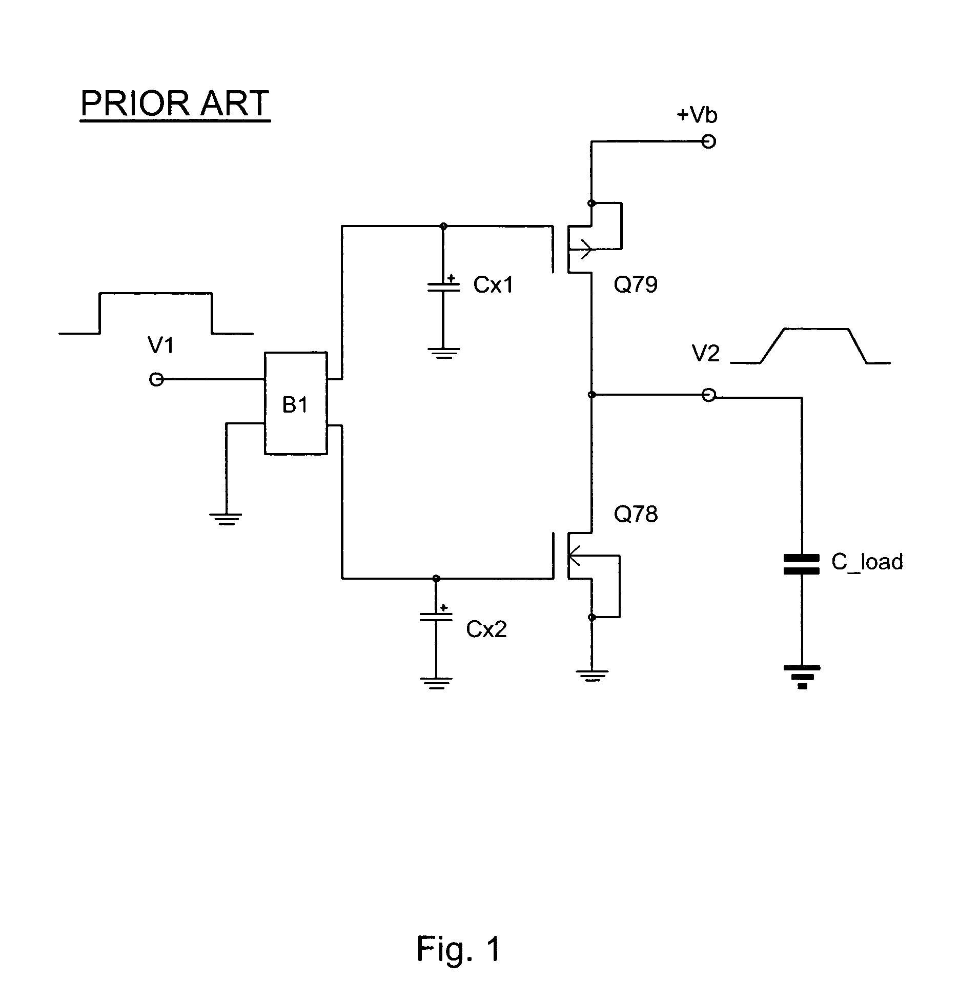
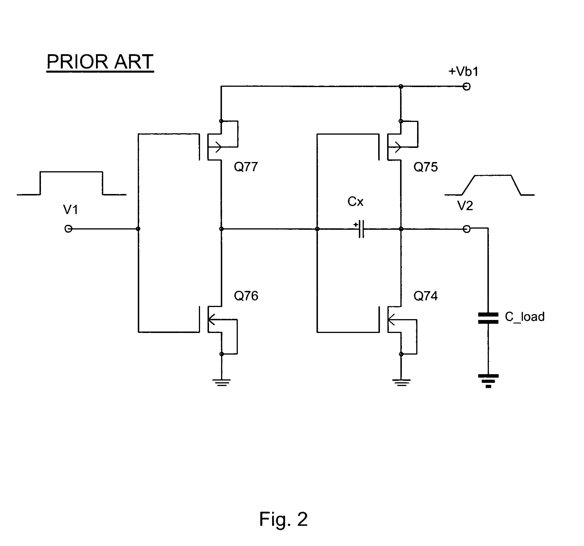
A further problem is that all the above solutions works reasonably well only if the load is capacitive (or resistive).
Therefore the above circuit solutions do not work as they should.
Furthermore the signal causes considerable interferences to a large spectrum (as shown for example in FIG. 6).
Yet furthermore the signal may interfere the reception and transmission channels of the mobile station and e.g. GPS reception.

Method used


Image

  • Circuit and apparatus for reducing interference of digital signals
  • Circuit and apparatus for reducing interference of digital signals
  • Circuit and apparatus for reducing interference of digital signals

Examples


Embodiment Construction

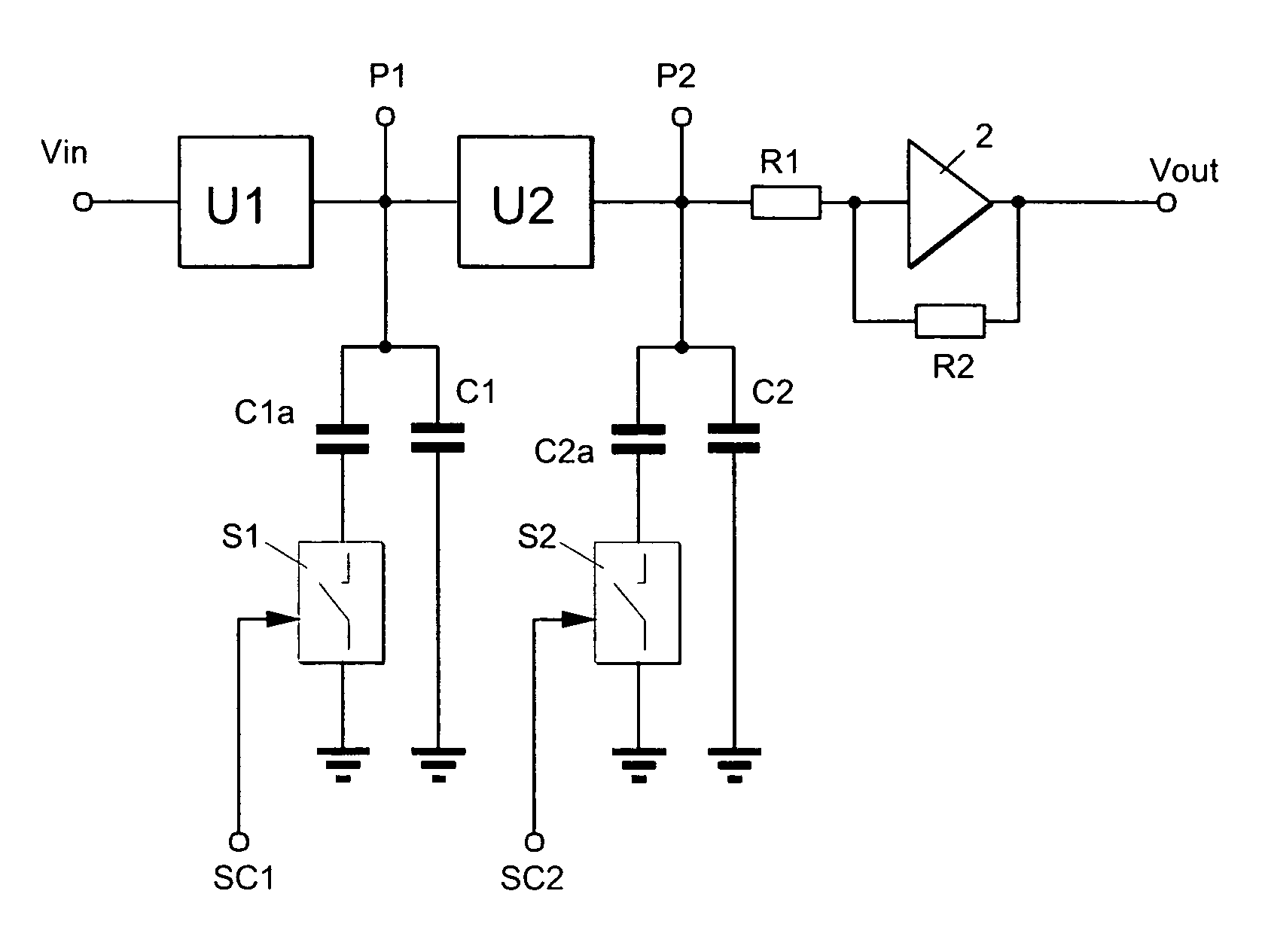
[0040]Various embodiments of the invention disclose a circuit and an apparatus, by which a digital pulse or the digital signal can be modified into a form, which has few harmonics. Furthermore the digital signal can be maintained clear while inputting to the stripline and to the impedance established by a capacitance.

[0041]If the digital signal is desired to be modified into such a form that interference is significantly reduced, the digital pulse should not have sharp or quick turnover, i.e. corners in the falling and rising edges. Thus too rapid transition points or turnovers should be avoided. The output stage should be able to feed the digital signal to the load, which is mainly formed by a lengthy stripline on the circuit board and the input capacitance of the following circuit.

[0042]FIG. 7 depicts a circuit for reducing the interference in accordance with various embodiments of the invention. The circuit is input by generally unmodified input signal Vin. Further embodiments of...


PUM


Abstract

A circuit for rounding the edges of a digital pulse so as to reduce interference has a first rounding block, a second rounding block and an output stage. The first rounding block rounds the second and fourth pulse edges so as to prolong rising and falling time of the digital pulse. The second rounding block rounds the first and third pulse edges in accordance with non-linear characteristics of a semiconductor of the second rounding block. The output stage is a feedback circuit where the first rounding block is coupled with the second rounding block and the second rounding block is coupled with the feedback circuit.

Description

TECHNICAL FIELD OF THE INVENTION[0001]The invention concerns a circuit for reducing interference of a digital signal. Furthermore the invention concerns an apparatus comprising the circuit and the use of the circuit and the apparatus.BACKGROUND OF THE INVENTION[0002]Digital signal based apparatuses, such as mobile stations, mobile phones or the like, use high clock frequencies and frequencies of the digital buses. The frequencies have increased all the time. Due to the high frequency also the interference, i.e. radio interference, increases. This is mainly because the rising and falling times of the high frequency digital signals cannot be increased to the same extent than the rising and falling times of the digital signal when using lower frequencies. A known solution so far for the worst interference problems has been based on a frequency planning. Thus it has been pursued to find such clock frequencies and bus frequencies where there are no harmonics or mixing of frequencies at t...

Claims


Application Information

Patent Timeline
Patent Type & Authority Patents(United States)
IPC IPC(8): H03K17/16
CPCH03K5/06H03K17/163H03K17/6872H03K19/00361H03K17/6874H03K2005/00071H03K2005/00156
Inventor VAISANEN, RISTO
Owner NOKIA CORP
Learn More