Apparatus and method for supplying voltage in semiconductor device

a technology of semiconductor devices and devices, applied in digital storage, automatic control, instruments, etc., can solve the problems of voltage drop, voltage drop, and voltage supply level of voltage supply units, and achieve the effect of deteriorating the performance of semiconductor devices

Active Publication Date: 2009-11-10
SAMSUNG ELECTRONICS CO LTD
View PDF5 Cites 0 Cited by
  • Summary
  • Abstract
  • Description
  • Claims
  • Application Information

AI Technical Summary

Benefits of technology

[0012]Accordingly, the present invention conducts an auxiliary current from / to a supply node to prevent voltage overshoot.
[0023]In this manner, the auxiliary current conducted from the supply node prevents a voltage overshoot at the supply node before the main current consuming units begin to conduct current. Thus, a stable voltage is generated at the supply node.

Problems solved by technology

However, when the current consuming units 120-1, 120-2, and 120-3 begin to consume a large quantity of current, the level of voltage supplied from the voltage supply unit 110 is lowered to result in a voltage drop.
Such a voltage drop may deteriorate the performance of the semiconductor device especially for high speed operation.
However, the internal voltage generator may provide excess current before such an operating time point to result in voltage overshoot which may also deteriorate the performance of the semiconductor device.
However, such increase of the power capacitance 130 undesirably results in increased size of the semiconductor device.

Method used


Image

  • Apparatus and method for supplying voltage in semiconductor device
  • Apparatus and method for supplying voltage in semiconductor device
  • Apparatus and method for supplying voltage in semiconductor device

Examples


Embodiment Construction

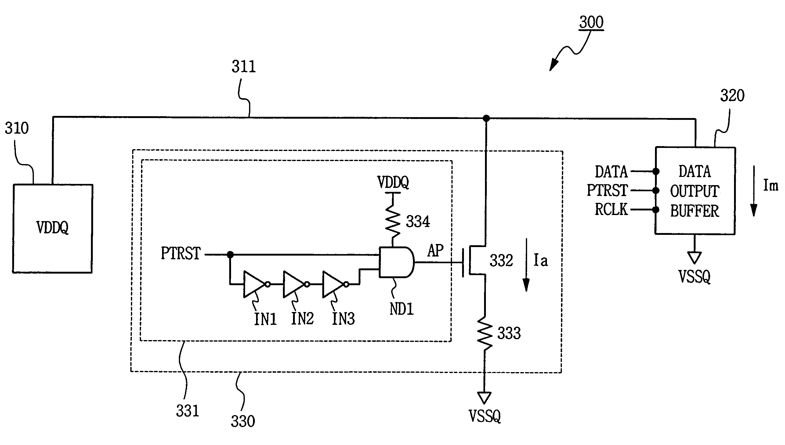
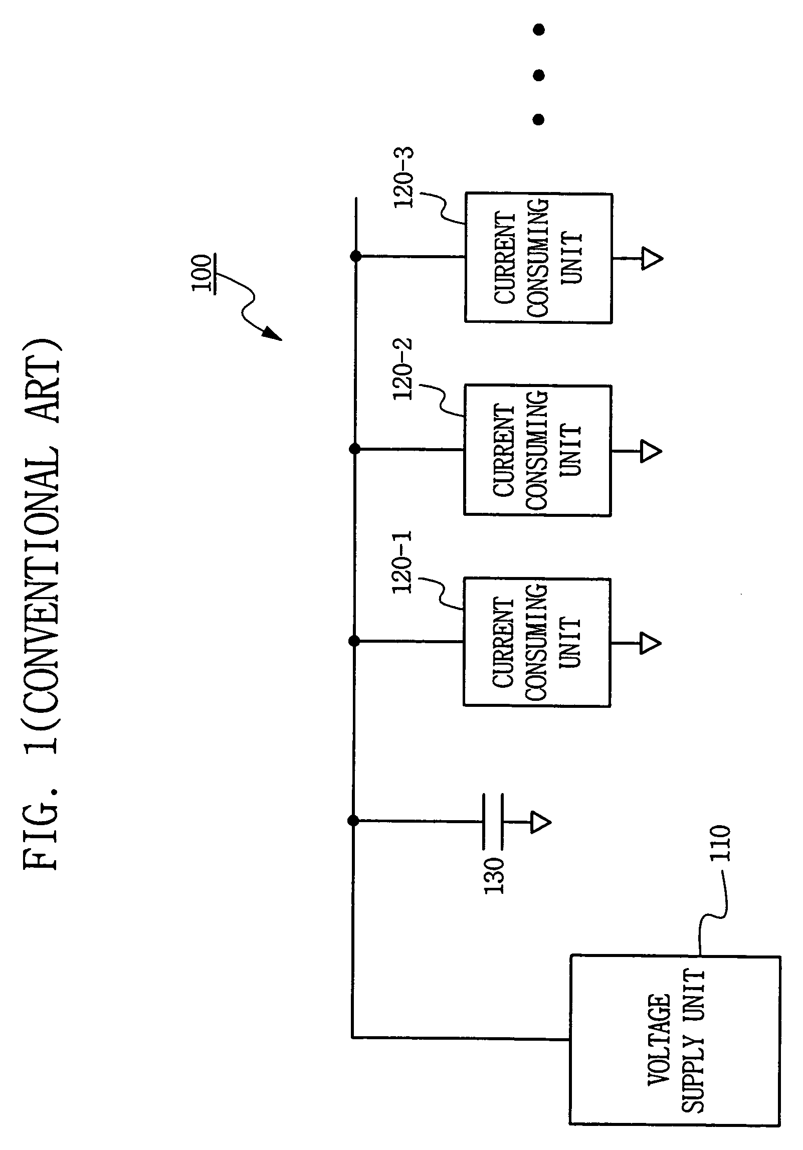
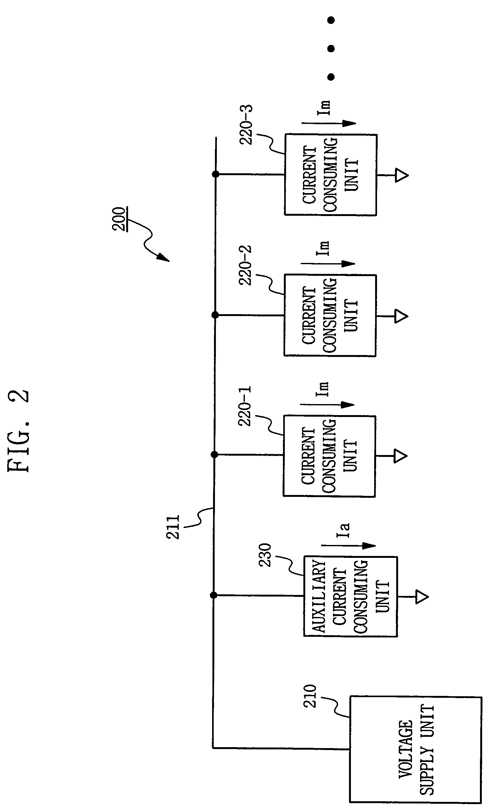
[0032]FIG. 2 shows a block diagram of a voltage supply apparatus for supplying a voltage within a semiconductor device 200 according to an embodiment of the present invention. The voltage supply apparatus includes a voltage supply unit 210 and an auxiliary current consuming unit 230, both coupled to a supply node 211.

[0033]The voltage supply apparatus of FIG. 2 provides a voltage applied at the supply node 211. A plurality of main current consuming units 220-1, 220-2, and 220-3 of the semiconductor device 200 are coupled to the supply node 211. The main current consuming units 220-1, 220-2, and 220-3 are components for performing typical operations of the semiconductor device 200. Each of the main current consuming units 220-1, 220-2, and 220-3 consumes a respective main current Im during such operation.

[0034]The voltage supply unit 210 is a pad having the voltage supplied from an external circuit applied thereon, in one example embodiment of the present invention. Alternatively, th...


PUM


Abstract

For supplying voltage to at least one main current consuming unit, a voltage supply unit provides the voltage to the at least one main current consuming unit at a supply node. In addition, an auxiliary current consuming unit conducts auxiliary current from / to the supply node for at least a predetermined time period before the at least one main current consuming unit begins to conduct current. Thus, voltage overshoot is prevented at the supply node.

Description

[0001]This application claims priority to Korean Patent Application No. 2006-03831, filed on Jan. 13, 2006 in the Korean Intellectual Property Office, the disclosure of which is incorporated herein in its entirety by reference.BACKGROUND OF THE INVENTION[0002]1. Field of the Invention[0003]The present invention relates generally to supplying voltage in a semiconductor device, and more particularly, to conducting an auxiliary current at a supply node to prevent a voltage spike at the supply node for supplying a stable voltage.[0004]2. Description of the Related Art[0005]In general, an electronic device operates with a voltage externally supplied as a power source. In particular, a semiconductor device includes internal voltage generators that generate internal voltages that are each higher or lower than the externally provided voltage to perform operations. For example, a semiconductor memory device generates write / read voltages from an externally supplied voltage for performing writ...

Claims


Application Information

Patent Timeline
Patent Type & Authority Patents(United States)
IPC IPC(8): H03L7/00
CPCH03K5/08G11C5/145G11C5/148G11C7/06G11C7/10G11C8/08
Inventor LEE, DONG-HYUK
Owner SAMSUNG ELECTRONICS CO LTD
Why Eureka
Try Eureka