Solid-state image pickup device and camera using the same
a pickup device and solid-state image technology, applied in the field of solid-state image pickup devices and cameras using the same, can solve problems such as delay in output time, and achieve the effects of reducing outputs from pixels, reducing gain, and suppressing the lik
- Summary
- Abstract
- Description
- Claims
- Application Information
AI Technical Summary
Benefits of technology
Problems solved by technology
Method used
Image

Examples
first embodiment
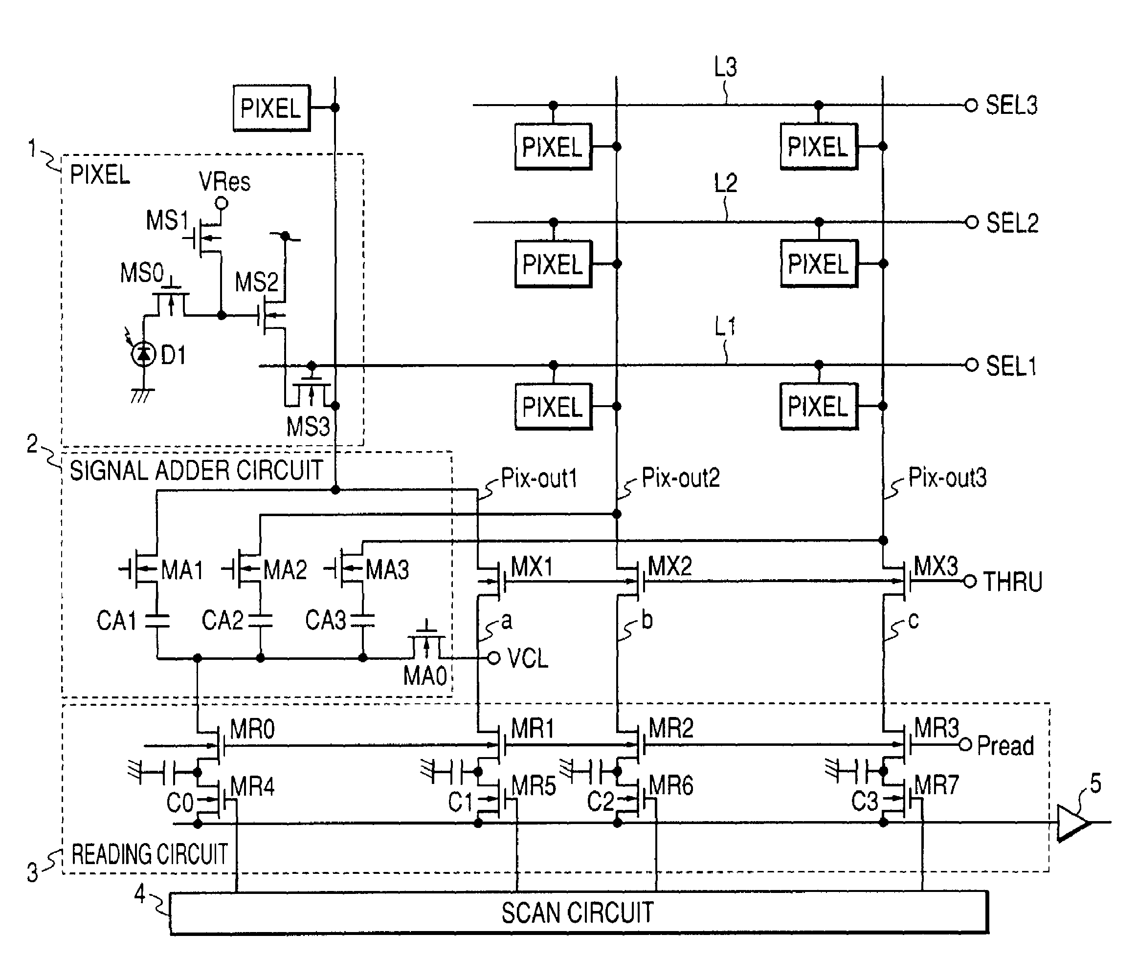
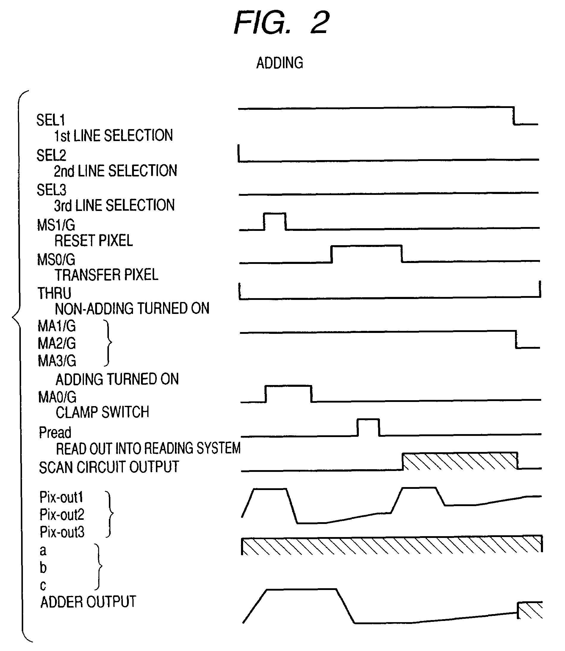
[0026]FIG. 1 is a diagram showing the invention most preferably and is a circuit diagram showing a partial construction of a solid-state image pickup device of the first embodiment. The construction shown in FIG. 1 shows a partial region (a region constructed by pixels of a 3×3 matrix configuration) of a pixel unit of a solid-state image pickup device shown in FIG. 10 and a signal adder circuit+non-adder circuit (for example, an individual signal output circuit), a reading circuit, and a scan circuit of such a partial region. The solid-state image pickup device shown in FIG. 10 is constructed by: a plurality of pixel units in each of which pixels are two-dimensionally arranged; a scan circuit 4′ for controlling a plurality of pixels in every row of the pixel unit; a signal adder circuit+non-adder circuit; a reading circuit 3; a scan circuit 4; and an output amplifier 5 (not shown).
[0027]Although the example in which the pixels are two-dimensionally arranged will be described in the ...
second embodiment
[0042]FIG. 4 is a circuit diagram showing a partial construction of a solid-state image pickup device according to the second embodiment of the invention.
[0043]Although its fundamental construction and the operation are similar to those in the first embodiment, the second embodiment differs from the first embodiment with respect to a point that a pixel 12 does not transfer the signal and a signal adder circuit 22 executes an adding (averaging) process by using a capacitance division.
[0044]The pixel 12 is constructed by the photodiode D1 and the MOS transistors MS1, MS2, and MS3. As compared with the pixel 1 in FIG. 1, the MOS transistor MS0 is deleted and the signal charges from the photodiode D1 are sent to the gate portion of the output transistor MS2 and its floating capacitor (FD).
[0045]The signal adder circuit 22 is constructed by: the switch transistors MA1 to MA3; three capacitors which are connected to the common output lines Pix−out1, Pix−out2, and Pix−out3 through the swit...
third embodiment
[0047]FIG. 5 is a circuit diagram showing a partial construction of a solid-state image pickup device according to the third embodiment of the invention.
[0048]Although its fundamental construction and the operation are similar to those in the first embodiment, the third embodiment differs from the first embodiment with respect to a point that after a signal adder circuit 23 executes addition (averaging) by using a capacitance division after the clamping. Since the signal addition in the row (horizontal) direction can be executed by a clamp circuit and the signal addition in the column (vertical) direction can be executed by a sampling and holding (S / H) circuit, a two-dimensional signal addition result can be obtained.
[0049]In the signal adder circuit 23, one terminal of the clamp capacitor CA1 is connected to the common output line Pix−out1 through the switch transistor MA1, one terminal of the clamp capacitor CA2 is connected to the common output line Pix−out2 through the switch tr...
PUM
 Abstract
Description
Claims
Application Information
 - R&D
- Intellectual Property
- Life Sciences
- Materials
- Tech Scout
- Unparalleled Data Quality
- Higher Quality Content
- 60% Fewer Hallucinations
Browse by: Latest US Patents, China's latest patents, Technical Efficacy Thesaurus, Application Domain, Technology Topic, Popular Technical Reports.
© 2025 PatSnap. All rights reserved.Legal|Privacy policy|Modern Slavery Act Transparency Statement|Sitemap|About US| Contact US: help@patsnap.com