
Image sensor with scaler and image scaling method thereof

a scaler and image sensor technology, applied in the field of cmos image sensors, can solve the problems of long image scaling time, small preview size of mobile phones or digital cameras, and limited operation speed of image sensors

Active Publication Date: 2009-09-15
INTELLECTUAL VENTURES II
View PDF10 Cites 12 Cited by
  • Summary
  • Abstract
  • Description
  • Claims
  • Application Information

AI Technical Summary

Benefits of technology

[0015]It is, therefore, an object of the present invention to provide an image sensor with an embedded scaling function and an image scaling method thereof, in which the scaling can be executed without any additional scaler chip.
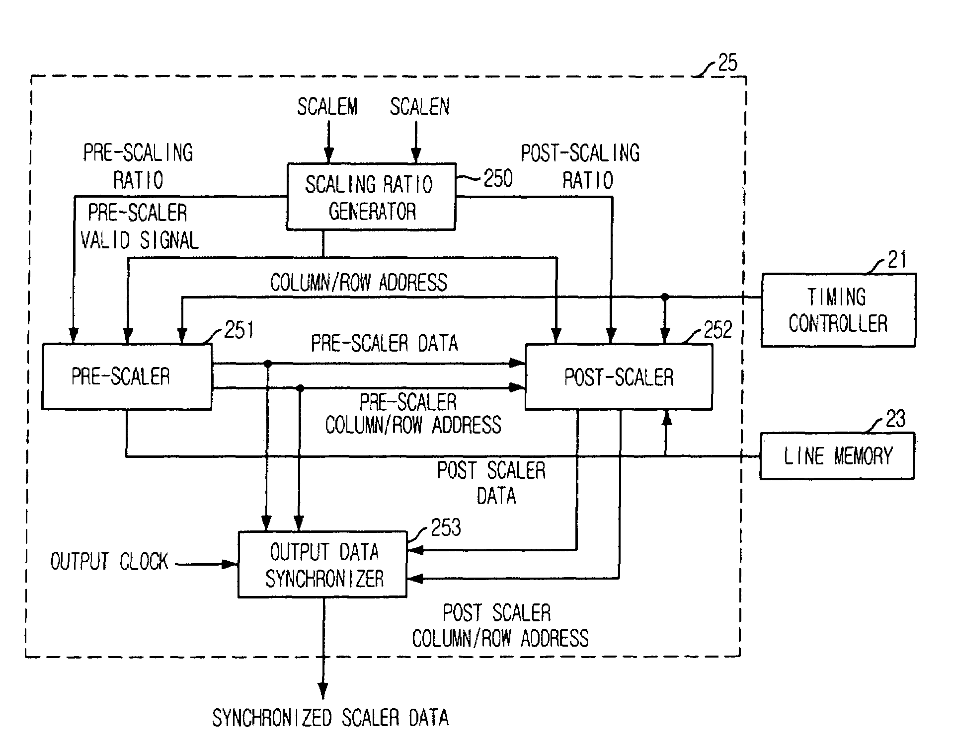
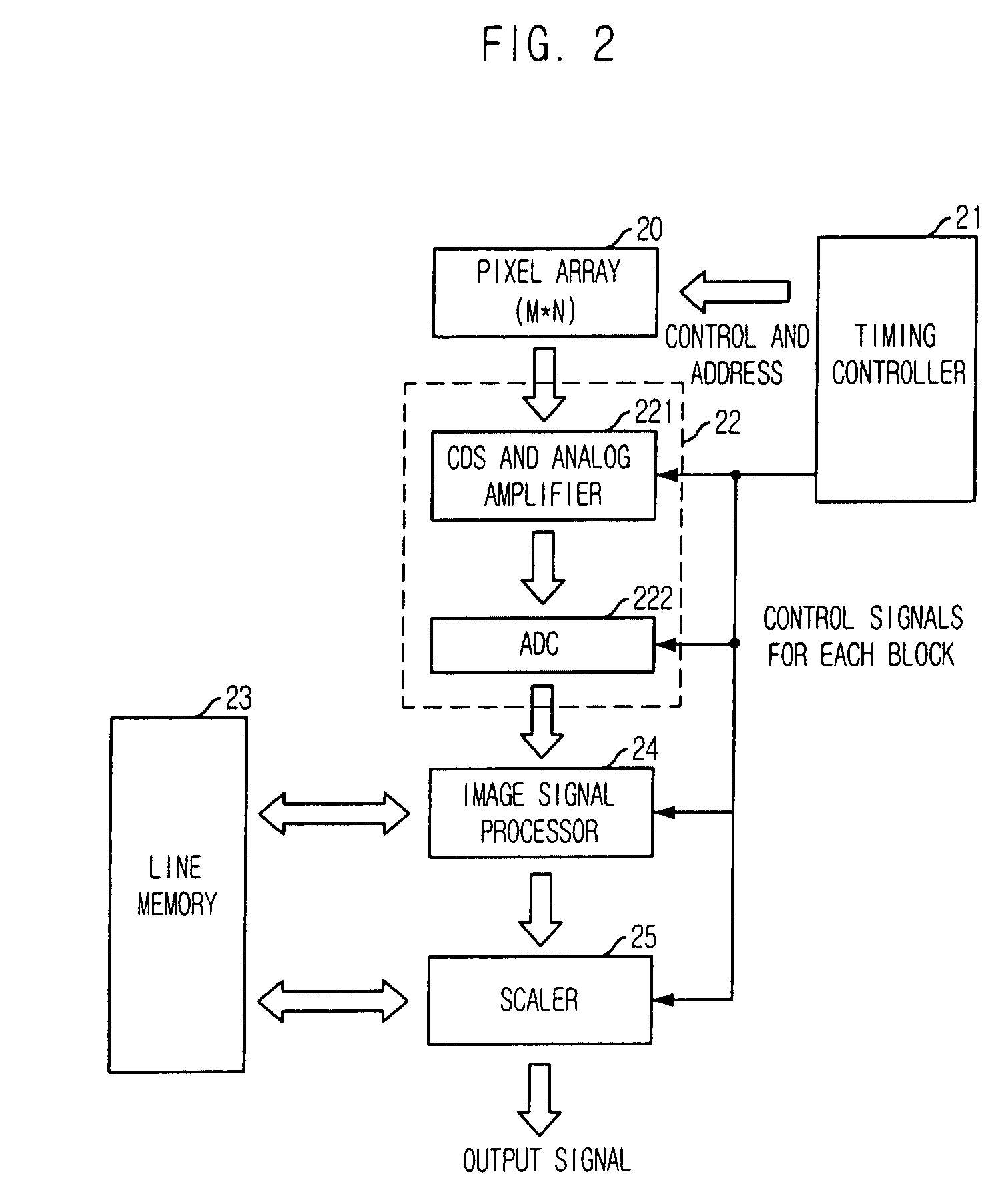
[0016]In accordance with an aspect of the present invention, there is provided an image sensor including: a pixel array having a plurality of pixels formed to maximize light sensing characteristic, the pixel array being configured to detect information on an external image; a timing controller for controlling an overall operation of the image sensor; an analog signal processor for converting an analog signal from the pixel array into a corresponding digital signal under control of the timing controller; a line memory for storing the digital signal in line unit; an image signal processor for processing a plurality of images by using the digital signal stored in the line memory so as to improve performance of the image sensor; and a scaler for receiving a scaling factor of a desired image size from the timing controller and calculating a scaling ratio so as to adjust an image size, and generating a corresponding row / column address and data and scaling the image stored in the line memory, whereby the image with the desired size is outputted.

Problems solved by technology

However, a preview size of a mobile phone or digital camera should be small because of a display limitation.
Therefore, a long time is taken for the image scaling.
An operation speed of the image sensor is limited due to the speed of the image scaling processed by the back-end chip.

Method used


Image

  • Image sensor with scaler and image scaling method thereof
  • Image sensor with scaler and image scaling method thereof
  • Image sensor with scaler and image scaling method thereof

Examples


Embodiment Construction

[0031]An image sensor with a scaler and an image scaling method thereof in accordance with exemplary embodiments of the present invention will be described in detail with reference to the accompanying drawings.

[0032]FIG. 2 is a block diagram of a CMOS image sensor in accordance with an embodiment of the present invention.

[0033]Referring to FIG. 2, the CMOS image sensor includes a pixel array 20 with M×N unit pixels (M and N are positive integers), a timing controller 21, an analog signal processor 22, an image signal processor 24, a line memory 23, and a scaler 25.

[0034]The analog signal processor 22 is provided with a CDS and analog amplifier 221, and a CDS 222.

[0035]The timing controller 21 is called a control and external system interface. The timing controller 11 controls an overall operation of the image sensor using an FSM and serves as an interface for an external system. Also, since the timing controller 21 has a batch register, it can program contents related to several int...


PUM


Abstract

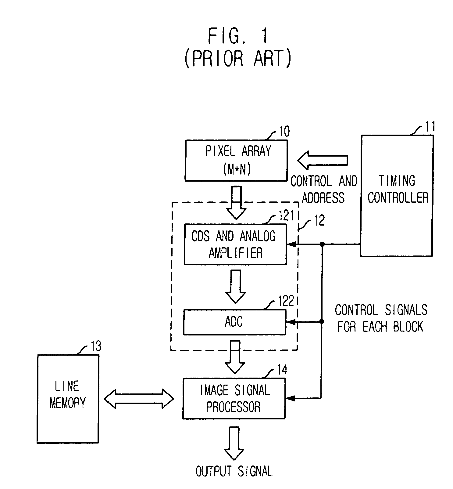
An image sensor is widely used in many fields, including the medical field and the security device field. Specifically, the image sensor is most widely used in digital cameras and mobile phones. The digital camera and the mobile phone require capturing images of higher resolution and higher quality. However, a preview size of the mobile phone or digital camera should be small because of a display limitation. Therefore, a function for reducing an image size or magnifying a specific portion of the picture is essential in the image sensor. Accordingly, there is provided an image sensor with a scaler. The image sensor with the scaler can arbitrarily adjust a size of an image without any additional scaling chip.

Description

CROSS REFERENCE TO RELATED APPLICATION[0001]The present application claims priority to and the benefit of Korean patent application No. KR 2005-0015506, filed in the Korean Patent Office on Feb. 24, 2005, the entire content of which is incorporated herein by reference.FIELD OF THE INVENTION[0002]The present invention relates to a CMOS image sensor; and, more particularly, to a CMOS image sensor with a scaler and an image scaling method thereof.DESCRIPTION OF THE RELATED ART[0003]An image sensor is an apparatus to capture images using light sensing semiconductor materials. Since brightness and wavelength of light from an object are different in their amount according to the reflection area, electrical signals from pixels are different from one another. These electrical signals are converted into digital signals, which can be processed in a digital circuit.[0004]FIG. 1 is a block diagram of an image sensor.[0005]Referring to FIG. 1, the image sensor includes a pixel array 10 with M×N ...

Claims


Application Information

Patent Timeline
Patent Type & Authority Patents(United States)
IPC IPC(8): G09G5/00H04N5/232H04N5/335H04N5/369H04N5/374H04N5/376H04N5/378H04N9/07
CPCH04N5/2628H04N5/23296H04N1/40068H01L27/146H04N23/69H04N23/12H04N25/75G06F3/14G06F3/0481G09G5/00G09G5/373G06T3/40G09G2360/02G06F15/7842G09G2340/0407
Inventor AHN, HYUN-JOO
Owner INTELLECTUAL VENTURES II
Learn More