Printed wiring board and process for manufacturing the same

a technology of printed wiring boards and manufacturing processes, applied in the direction of printed circuit non-printed electric components association, sustainable manufacturing/processing, final product manufacturing, etc., can solve the problems of insufficient short insulation distance, inability to achieve high-density mounting, and inability to reduce the size of printed wiring boards, etc., to achieve low cost

Inactive Publication Date: 2009-09-08
YAZAKI CORP
View PDF15 Cites 5 Cited by
  • Summary
  • Abstract
  • Description
  • Claims
  • Application Information

AI Technical Summary

Benefits of technology

[0015]It is therefore an objective of the present invention to solve the above problems and to provide a printed wiring board and a process for manufacturing a printed wiring board, by which the electrical insulation between the solder lands, on which the components to be mounted are mounted, can be securely attained with a low cost.
[0017]With the construction described above, by providing the first insulating layer, a step between the peripheral part of the solder land and the board becomes small and an edge of the peripheral part becomes round, therefore a thickness of the second insulating layer to be piled up on the first insulating layer can be set large. Thereby, electrical insulation between the solder lands can be clearly ensured and a flux of the solder can be securely prevented from spreading beyond the second insulating layer to the outside of the solder land. Therefore, the electrical insulation between the solder lands, on which electric components are mounted, can be ensured with low cost and with a small size construction.
[0019]With the construction described above, the second insulating layer also can be formed when a terminal number and electric component number are printed on the board by silk-screen printing, therefore the electrical insulation between the solder lands, on which electric components are mounted, can be ensured with low cost and without increasing manufacturing steps.
[0021]With the construction described above, the step, in which the component to be mounted is mounted on the central part of the one solder land and electrically connected to the one solder land by solder, is carried out after the step, in which the second insulating layer is formed by piling up on the first insulating layer which covers the portion of the peripheral part of the one solder land. Therefore, a flux of the solder can be securely prevented from spreading beyond the second insulating layer to the outside of the solder land. Therefore, the electrical insulation between the solder lands, on which electric components are mounted, can be ensured with low cost.

Problems solved by technology

However, the distance L must be a certain length so as to secure electrical insulation, which causes a problem that a size of the printed wiring board cannot be decreased.
However, in this case, it is not possible to provide the electric component 14 on the rear side of the electric components 12 and 13 because of the hole 19, causing a problem that a high-density mounting cannot be realized.
However, there is a possibility that the flux residue 18 takes place on the silk 20, causing a problem.
Further, since there is a possibility that a pin-hole takes place on the resist film 17, a short insulation distance cannot be sufficiently attained even if the step is provided.
However, it is very difficult to form a thick resist film 17 with a general method and there is a problem in terms of a cost.
However, there has been no proposal as to a method of attaining electrical insulation between the solder lands 16.

Method used


Image

  • Printed wiring board and process for manufacturing the same
  • Printed wiring board and process for manufacturing the same
  • Printed wiring board and process for manufacturing the same

Examples


Embodiment Construction

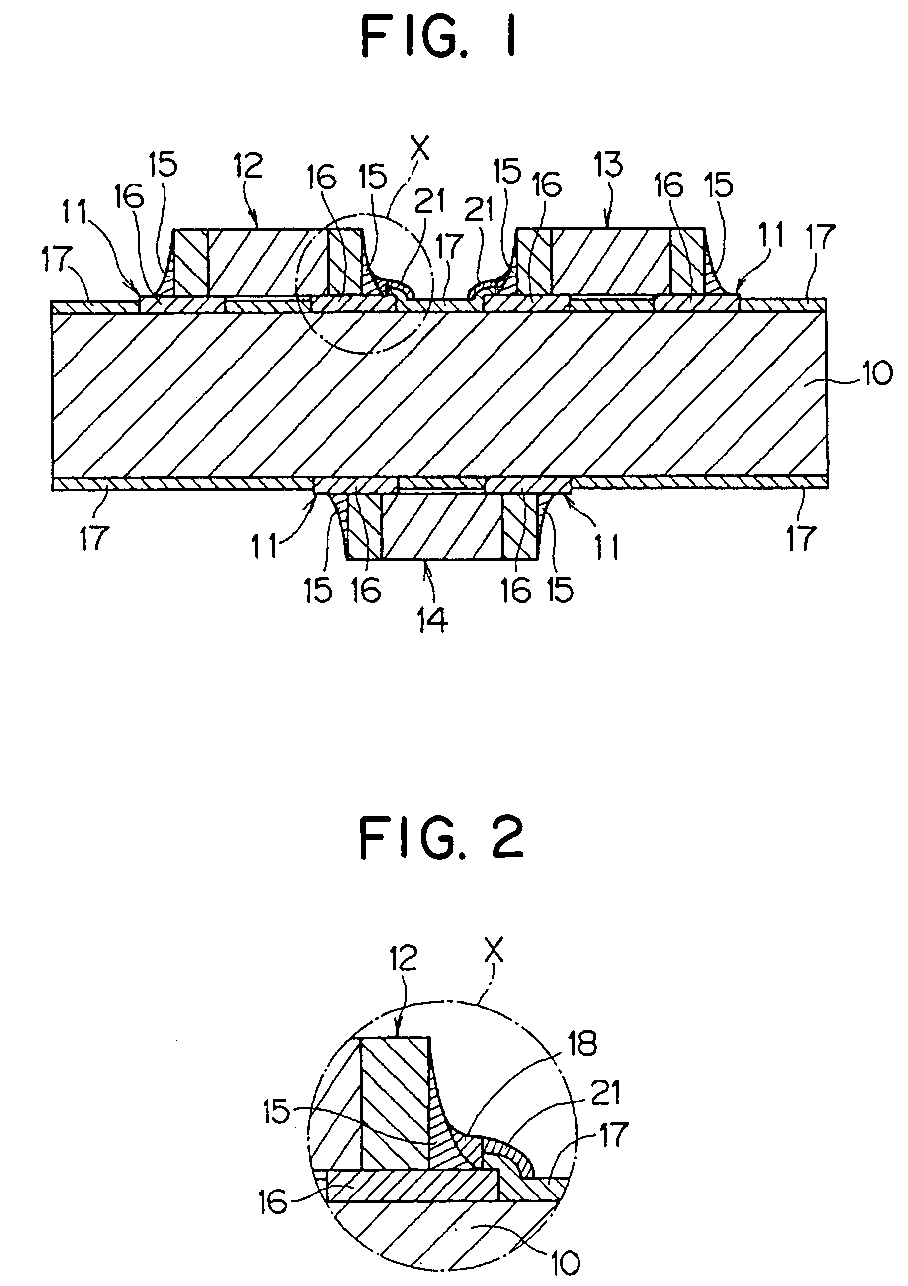
[0030]In the following, a preferred embodiment of the present invention will be explained with reference to the attached drawings.

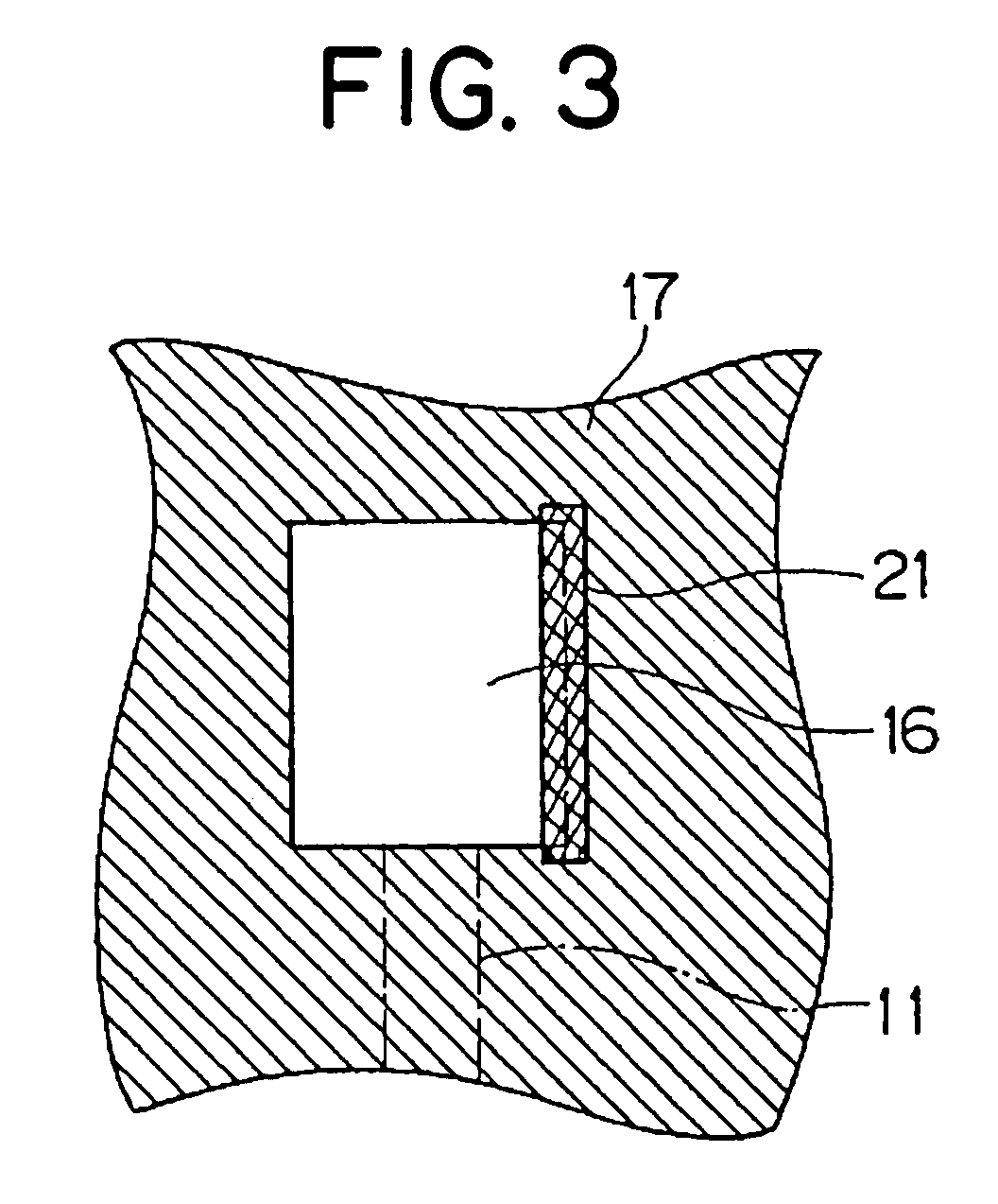
[0031]As shown in FIGS. 1-3, a printed wiring board includes a board 10 and a conductive wiring 11 formed on a top surface and an under surface of the board 10. The conductive wiring 11 includes solder lands 16 to which a plurality of components 12, 13, 14 to be mounted are electrically connected by solder 15. The solder land 16 is formed wider than the other part of the conductive wiring 11 so that the soldering is carried out easily.

[0032]The components 12, 13 are arranged on the side of the top surface of the board 10. The components 12, 13 are arranged near to each other and must be electrically insulated from each other. The component 14 is arranged on the side of the under surface of the board 10. There is no other component to be mounted being arranged in the proximity of the component 14, from which other component the component 14 must be electri...


PUM


Abstract

The printed wiring board includes: a conductive wiring which is formed on a surface of a board and has a plurality of solder lands, to which components to be mounted are electrically connected by solder; and first and second electrically insulating layers formed on the conductive wiring, wherein the first insulating layer is formed on the conductive wiring in such a manner that the first insulating layer covers a portion of a peripheral part of one solder land and a central part of the one solder land is exposed, the portion of the peripheral part being situated on the side of another solder land, wherein the second insulating layer is piled up on the first insulating layer which covers the portion of the peripheral part of the one solder land.

Description

BACKGROUND OF THE INVENTION[0001](1) Field of the Invention[0002]The present invention relates to a printed wiring board and a process for manufacturing a printed wiring board, in particular, a printed wiring board including: a conductive wiring, which is formed on a surface of a board and has a solder land to which components to be mounted are electrically connected by solder; and a first electrically insulating layer formed on the conductive wiring, and a process for manufacturing such a printed wiring board.[0003](2) Description of the Related Art[0004]As an example of a conventional printed wiring board, for example, a printed wiring board shown in FIG. 5 has been proposed. As shown in FIG. 5, the printed wiring board includes a board 10 and a conductive wiring 11 formed on a surface of the board 10. The conductive wiring 11 includes solder lands 16, to which electric components 12, 13, 14 are electrically connected by solder 15.[0005]A resist film 17 as the first insulating lay...

Claims


Application Information

Patent Timeline
Patent Type & Authority Patents(United States)
IPC IPC(8): H05K7/10
CPCH05K3/3442H05K3/3452Y10T29/49144H05K2201/10636H05K2203/0588H05K2201/099Y02P70/50
Inventor KAWAMURA, YOSHIHIRO
Owner YAZAKI CORP
Why Eureka
Try Eureka