
Etch singulated semiconductor package

a semiconductor and singulated technology, applied in semiconductor devices, semiconductor/solid-state device details, electrical equipment, etc., can solve the problems of premature wear of the costly saw singulated blade, cutting through copper with the saw blade, and the lead of the separated leadframes being burrowed, etc., to achieve the effect of reducing costs

Inactive Publication Date: 2009-03-24
AMKOR TECH SINGAPORE HLDG PTE LTD
View PDF399 Cites 36 Cited by
  • Summary
  • Abstract
  • Description
  • Claims
  • Application Information

AI Technical Summary

Benefits of technology

The present invention provides methods for making multiple semiconductor packages simultaneously using etching techniques instead of traditional cutting methods like sawing or punching. This results in lower costs and fewer defects.

Problems solved by technology

One of the drawbacks associated with the saw singulation process used in relation to the manufacture of semiconductor packages is that the saw blade used in the saw singulation process cuts through copper (i.e., the metal material typically used to fabricate the strip) usually most of the time.
As will be recognized, this level of sawing through copper as occurs as a result of the configuration of the strip often results in the premature wear of the costly saw singulation blades.
Another drawback of the saw singulation process is that the same also typically results in the burring of the leads of the separated leadframes.
Saw generated burrs at the leads often adversely affect solder mounting and joint reliability.
However, as will be recognized, the use of the high cost saw blades is undesirable due to the resultant increase in production cost, with the reduced feed rates needed to control burring also adversely affecting production speed, and thus efficiency.
With particular regard to the punch singulation process, one of the drawbacks associated with the use of such process is the tendency for the hardened encapsulant material or package body of the semiconductor package to chip or crack as a result of the punching operation.
As will be recognized, such chipping or cracking of the package body can result in the accelerated failure thereof as a result of, among other things, moisture permeation to the embedded integrated circuit die.
Further, punch singulation is typically not preferred for applications using mechanically sensitive die due to the perceived risk associated with impact vibration (e.g., MEMS).

Method used


Image

  • Etch singulated semiconductor package
  • Etch singulated semiconductor package
  • Etch singulated semiconductor package

Examples


Embodiment Construction

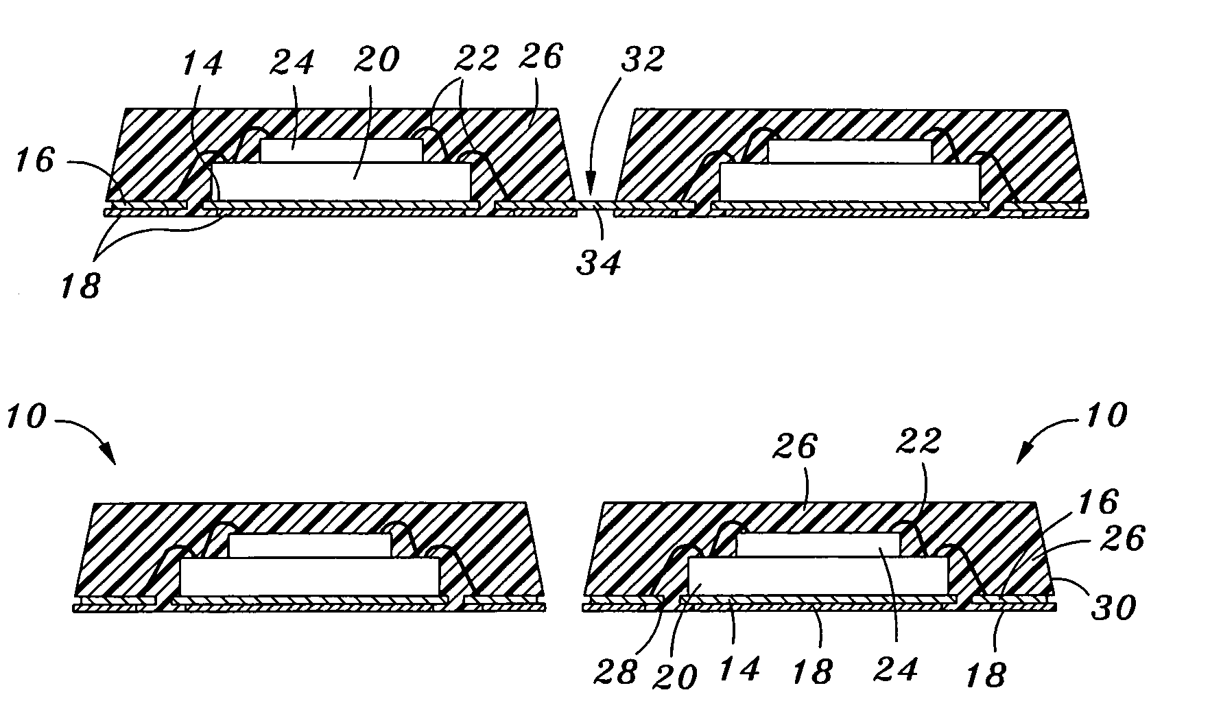
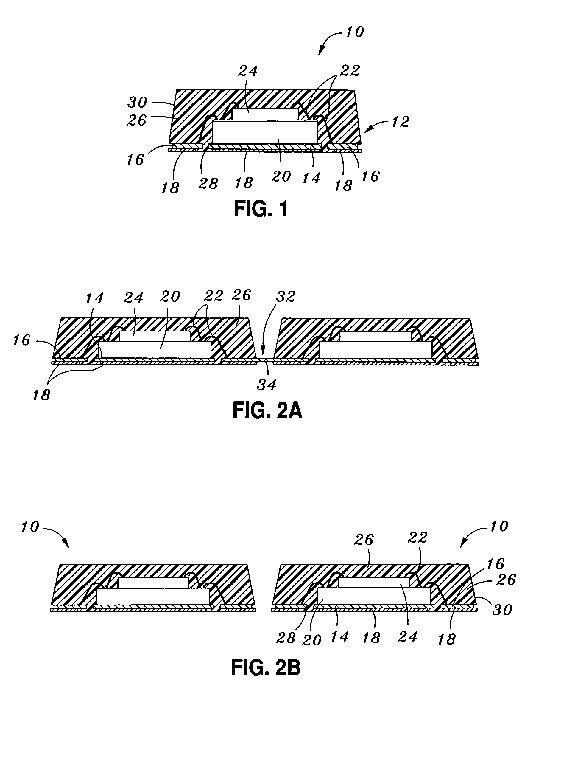
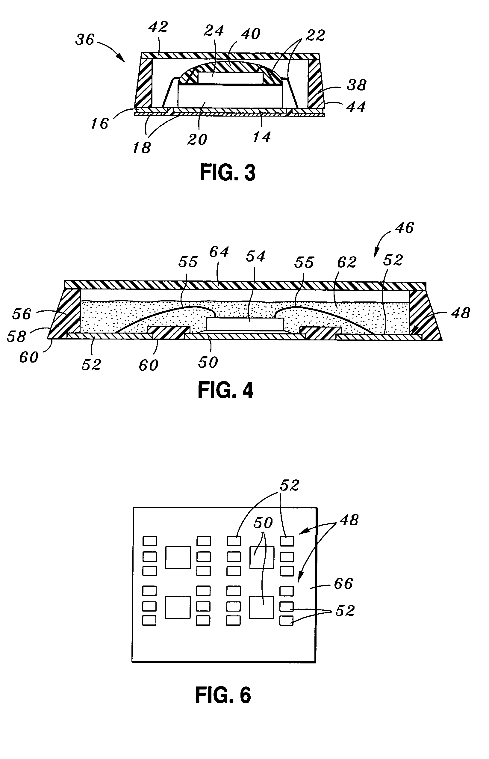
[0021]Referring now to the drawings where the showings are for purposes of illustrating various embodiments of the present invention only, and not for purposes of limiting the same, FIG. 1 illustrates a semiconductor package 10 constructed in accordance with one embodiment of the present invention. The semiconductor package 10 comprises a leadframe 12 which is preferably fabricated from a conductive metal material (e.g., copper). The leadframe 12 includes a die pad 14 which has a generally quadrangular (e.g., square, rectangular) configuration and defines opposed, generally planar top and bottom surfaces. In addition to the die pad 14, the leadframe 12 includes a plurality of leads 16. The leads 16 are typically segregated into multiple sets, with the leads 16 of each set extending along and in spaced relation to a respective one of the peripheral edge segments defined by the die pad 14. In this regard, the leadframe 12 of the semiconductor package 10 may be provided with one or mor...


PUM


Abstract

In accordance with the present invention, there is provided various methods of simultaneously fabricating a plurality of semiconductor packages (e.g., cavity type semiconductor packages) wherein the singulation process is achieved using etching techniques as opposed to more conventional cutting techniques such as sawing or punching. Such etching techniques are inherently lower in cost and free from many of the defects induced by other cutting techniques.

Description

CROSS-REFERENCE TO RELATED APPLICATIONS[0001]Not ApplicableSTATEMENT RE: FEDERALLY SPONSORED RESEARCH / DEVELOPMENT[0002]Not ApplicableBACKGROUND OF THE INVENTION[0003]The present invention relates generally to semiconductor package technology, and more particularly to a unique manufacturing methodology for a semiconductor package wherein singulation is accomplished by etching as opposed to mechanical cutting (e.g, sawing or punching).[0004]Integrated circuit dies are conventionally enclosed in plastic packages that provide protection from hostile environments and enable electrical interconnection between the integrated circuit die and an underlying substrate such as printed circuit board (PCB). The elements of such a package include a metal leadframe, an integrated circuit die, bonding material to attach the integrated circuit die to the leadframe, bond wires which electrically connect pads on the integrated circuit die to individual leads of the leadframe, and a hard plastic encapsu...

Claims


Application Information

Patent Timeline
Patent Type & Authority Patents(United States)
IPC IPC(8): H01L21/00
CPCH01L21/561H01L23/24H01L23/3107H01L23/315H01L23/49575H01L24/97H01L21/568H01L24/48H01L2224/48091H01L2224/73265H01L2224/97H01L2924/01027H01L2924/01029H01L2924/01046H01L2924/01075H01L2924/01078H01L2924/01079H01L2924/01082H01L2924/14H01L2924/16195H01L2924/01005H01L2224/85001H01L2924/1461H01L2924/01033H01L2924/01006H01L2224/32245H01L2224/48145H01L2224/48247H01L2224/83001H01L2924/00014H01L2224/85H01L2924/00H01L2224/8592H01L2924/181H01L2924/00012H01L2224/45099H01L2224/45015H01L2924/207
Inventor BERRY, CHRISTOPHER J.SCANLAN, CHRISTOPHER M.FAHEEM, FAHEEM F.
Owner AMKOR TECH SINGAPORE HLDG PTE LTD
Learn More