Optically compensated birefringence liquid crystal display panel

a liquid crystal display and birefringence technology, applied in static indicating devices, instruments, non-linear optics, etc., can solve the problems of signal delay, increase the consumption power of the driver ic, and disadvantage of the “instant on” characteristic of the lcd. achieve the effect of speeding up the transition

Active Publication Date: 2009-03-03
AU OPTRONICS CORP
View PDF5 Cites 2 Cited by
  • Summary
  • Abstract
  • Description
  • Claims
  • Application Information

AI Technical Summary

Benefits of technology

[0013]Accordingly, the present invention is directed to provide an optically compensated birefringence liquid crystal display (LCD) panel, which can speed up the transition of the optically compensated birefringence LCD panel from splay state to bend state through the electric field formed by the scan lines or the data lines with the electrode lines.
[0014]According to another aspect of the present invention, an optically compensated birefringence LCD panel is provided, which can resolve the problem of delay of data signal when a high voltage is supplied to the control signal electrode of the conventional LCD panel.
[0015]According to yet another aspect of the present invention, an optically compensated birefringence LCD panel is provided, which can resolve the problem of high power consumption of the driver IC of the conventional LCD panel.

Problems solved by technology

However, the optically compensated birefringence LCD can only enter standby status to provide quick response performance after all the liquid crystal molecules are switched from splay state to bend state.
However, this is very disadvantageous to the “instant on” characteristic of LCD.
However, since the data lines 113 are close to the control signal electrodes 116 supplied with a high voltage, thus, the data signal transmission in the data lines 113 are affected by load increase, which will further induce the problem of signal delay, and meanwhile, increase the consumption power of the driver IC.

Method used


Image

  • Optically compensated birefringence liquid crystal display panel
  • Optically compensated birefringence liquid crystal display panel
  • Optically compensated birefringence liquid crystal display panel

Examples


first embodiment

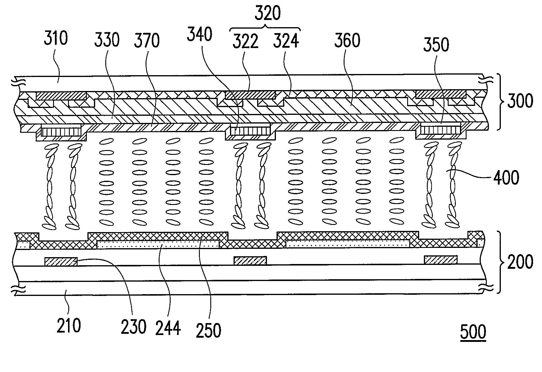
[0060]FIG. 2A is a cross-sectional view of an optically compensated birefringence LCD panel according to the first embodiment of the present invention, and FIG. 2B is a top view of an active device array apparatus in an optically compensated birefringence LCD panel in FIG. 2A, wherein the active device array apparatus in FIG. 2A is a cross-sectional view of FIG. 2B cut along line B-B′. Referring to both FIG. 2A and FIG. 2B, the optically compensated birefringence LCD panel 500 includes an active device array apparatus 200, a color filter apparatus 300, and an optically compensated birefringence liquid crystal layer 400 disposed between the active device array apparatus 200 and the color filter apparatus 300.

[0061]The active device array apparatus 200 includes a substrate 210, a plurality of scan lines 220, a plurality of data lines 230, and a plurality of pixel units 240. The scan lines 220, the data lines 230, and the pixel units 240 are all disposed on the substrate 210. Each pixe...

second embodiment

[0070]FIG. 3A is a cross-sectional view of an optically compensated birefringence LCD panel according to the second embodiment of the present invention, wherein the active device array apparatus of the optically compensated birefringence LCD panel in FIG. 3A is the same as the active device array apparatus in FIG. 2B. Referring to FIG. 3A, the optically compensated birefringence LCD panel 700 includes an active device array apparatus 200, a color filter apparatus 600, and an optically compensated birefringence liquid crystal layer 400 disposed between the active device array apparatus 200 and the color filter apparatus 600.

[0071]The active device array apparatus 200 and the optically compensated birefringence liquid crystal layer 400 are the same as those described in the first embodiment, so the details will not be described here again. The color filter apparatus 600 includes a substrate 310, a color filter array 320, a flat layer 610, a plurality of electrode patterns 620, and a p...

third embodiment

[0076]FIG. 4 is a cross-sectional view of an optically compensated birefringence LCD panel according to the third embodiment of the present invention, wherein the active device array apparatus of the optically compensated birefringence LCD panel in FIG. 4 is the same as the active device array apparatus in FIG. 2B. Referring to FIG. 4, the optically compensated birefringence LCD panel 900 includes an active device array apparatus 200, a color filter apparatus 800, and an optically compensated birefringence liquid crystal layer 400 disposed between the active device array apparatus 200 and the color filter apparatus 800.

[0077]The active device array apparatus 200 and the optically compensated birefringence liquid crystal layer 400 are the same as those described in the first embodiment, so details will not be described again. The color filter apparatus 800 includes a substrate 310, a color filter array 810, an insulating layer 820, a flat layer 830, and a plurality of electrode patte...


PUM

PropertyMeasurementUnit
voltageaaaaaaaaaa
voltageaaaaaaaaaa
voltageaaaaaaaaaa

Abstract

An optically compensated birefringence liquid crystal display (LCD) panel is provided, which includes an active device array apparatus, a color filter apparatus, and an optically compensated birefringence liquid crystal layer disposed between the active device array apparatus and the color filter apparatus. The color filter apparatus includes a substrate, a color filter array, a common electrode, a plurality of electrode lines, and an insulating layer. The color filter array is disposed on the substrate and has a black matrix and a color filter layer. The common electrode is disposed over the color filter array. The electrode lines are disposed over the common electrode. The insulating layer is disposed between the common electrode and the electrode lines. Accordingly, the problems of delay of data signal and overload of the driving circuit when a high voltage is applied to the control signal electrode of the conventional LCD panel are resolved.

Description

CROSS-REFERENCE TO RELATED APPLICATION[0001]This application claims the priority benefit of Taiwan application Ser. No. 95104694, filed on Feb. 13, 2006. All disclosure of the Taiwan application is incorporated herein by reference.BACKGROUND OF THE INVENTION[0002]1. Field of Invention[0003]The present invention relates to a liquid crystal display (LCD) panel. More particularly, the present invention relates to an optically compensated birefringence LCD panel having short response time.[0004]2. Description of Related Art[0005]Liquid crystal displays are divided into many categories based on the type of liquid crystal used, the driving method, and the location of light source disposition. Wherein, optically compensated birefringence liquid crystal display (OCB LCD) has very quick response speed and can provide more smooth display quality while playing fast-switching continuous images such as animations, so it is very suitable to be applied to high-scale LCD. However, the optically com...

Claims


Application Information

Patent Timeline
Patent Type & Authority Patents(United States)
IPC IPC(8): G02F1/1343
CPCG02F1/133514G02F1/1362G02F1/1395G02F2001/133565G02F2201/121G02F1/133565G02F1/13363
Inventor LIAO, CHI-NAN
Owner AU OPTRONICS CORP
Why Eureka
Try Eureka