Nanoscale content-addressable memory

a content-adressable memory and nano-scale technology, applied in static storage, digital storage, instruments, etc., can solve the problems of affecting the very advantage of nano-sized components, and unable to meet the needs of nano-sized components

Inactive Publication Date: 2009-02-24
UNIV OF FLORIDA RES FOUNDATION INC
View PDF9 Cites 8 Cited by
  • Summary
  • Abstract
  • Description
  • Claims
  • Application Information

AI Technical Summary

Problems solved by technology

A fundamental challenge remains, however, regarding how to interface nanometer-sized components to present micrometer sized devices.
Difficulties arise in achieving a satisfactory interface not only because of the scale mismatch, but also because conventional device techniques are based on miniaturizing a precise interconnect and device geometry (top down), while at the nanometer scale designers have to cope with less precise geometry and / or location of components.
One apparent difficulty with a MWCM is that a direct, one-to-one connection of its nanometer-sized input and output buses to a micrometer-sized component would likely consume more area on a chip than the MWCM itself, thus possibly undercutting the very advantage of the nanometer-sized component.
Currently available lithography techniques, however, can make unique addressing of each nanowire problematic.
Such an approach for a device comprising M microwires and N nanowires, however, requires M×N searches, which typically results in a large number of searches being performed.

Method used


Image

  • Nanoscale content-addressable memory
  • Nanoscale content-addressable memory
  • Nanoscale content-addressable memory

Examples


examples

[0121]The above analysis provides a foundation for understanding how each system parameter affects the performance. The following non-limiting examples are intended to convey further characteristics and advantages based on such analysis. The examples, however, are only illustrative. The are not intended to be exhaustive of the various ways of practicing the claimed invention, as will be readily apparent to one skilled in the art having the advantage of the teachings provided herein.

[0122]Moreover, the results are only an approximated and are not easily calculated or even estimated. Because of this, Monte-Carlo simulations were used as described below to calculate the performance for a particular set of parameters.

[0123]The performance of architecture according to the present invention was simulated by making the following assumptions about the electrical properties of the device: 1) the asymmetric junctions are diodes; 2) the resistance of the crossbar memory diodes dominates all ot...


PUM


Abstract

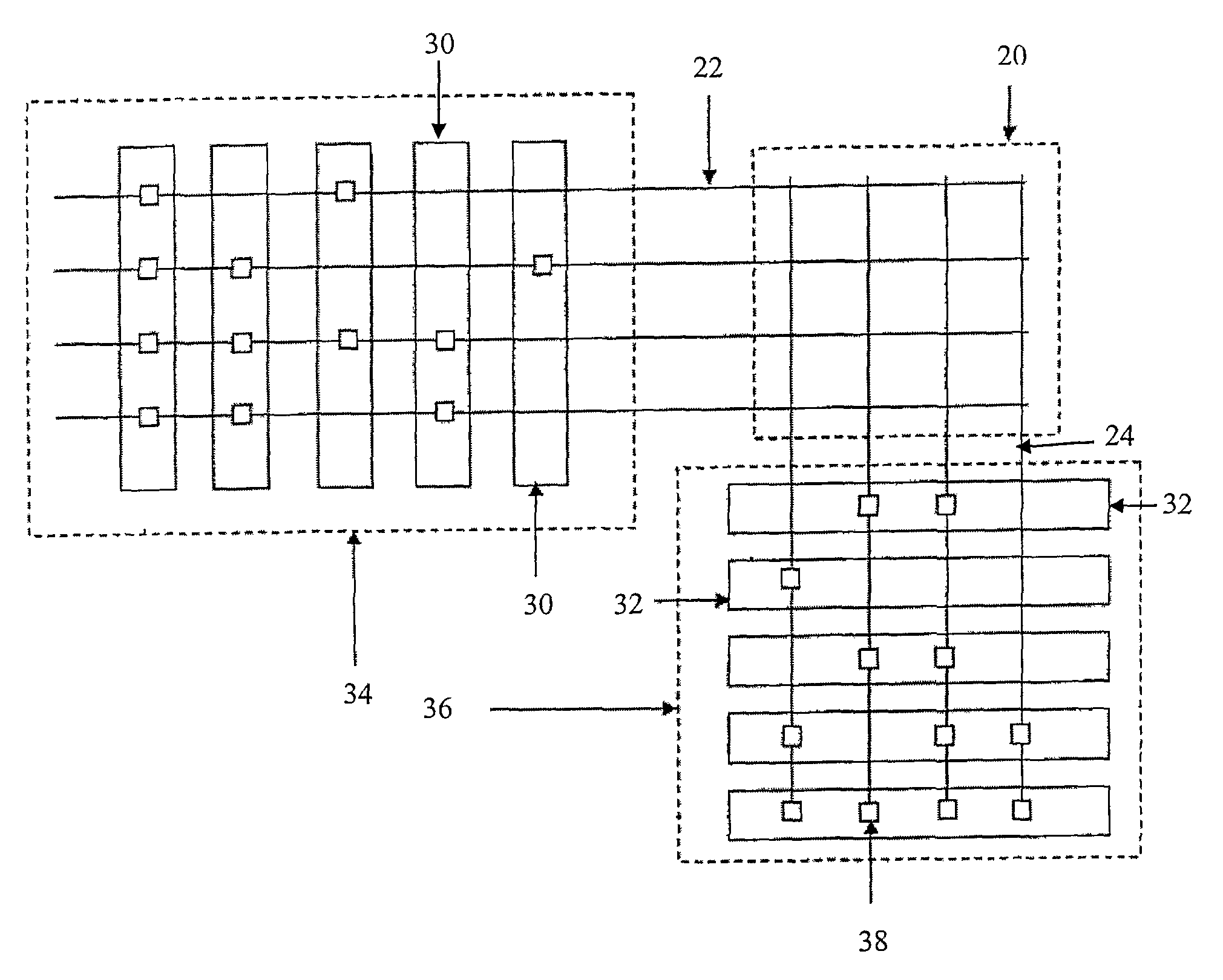
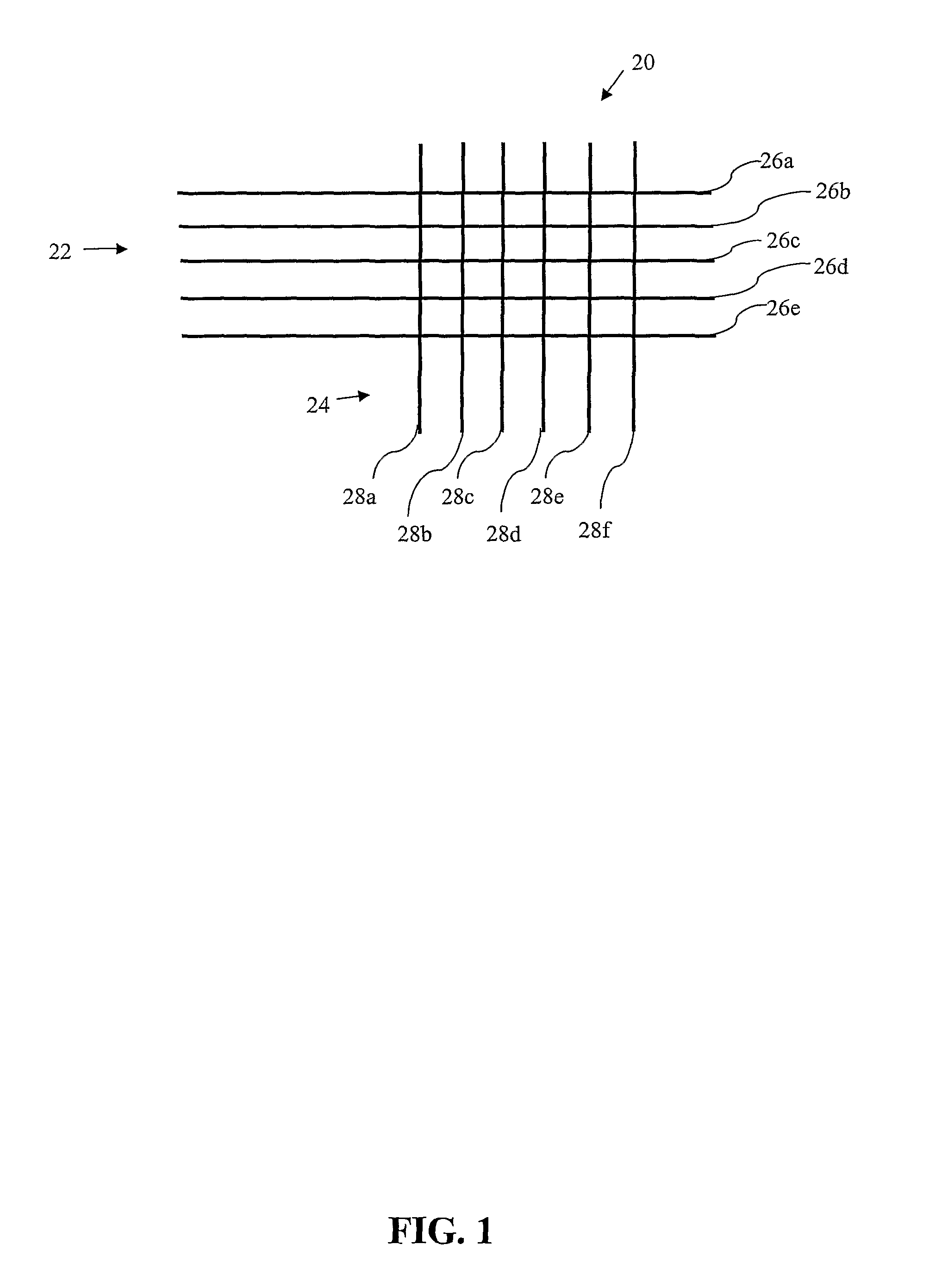
A combined content addressable memory device and memory interface is provided. The combined device and interface includes one or more one molecular wire crossbar memories having spaced-apart key nanowires, spaced-apart value nanowires adjacent to the key nanowires, and configurable switches between the key nanowires and the value nanowires. The combination further includes a key microwire-nanowire grid (key MNG) electrically connected to the spaced-apart key nanowires, and a value microwire-nanowire grid (value MNG) electrically connected to the spaced-apart value nanowires. A key or value MNGs selects multiple nanowires for a given key or value.

Description

CROSS-REFERENCE TO RELATED APPLICATIONS[0001]This application is a §371 national stage entry of International Application No. PCT / US2005 / 028928, filed Aug. 15, 2005, which claims priority to U.S. Provisional Application No. 60 / 601,347, filed Aug. 13, 2004, both of which are hereby incorporated by reference.STATEMENT REGARDING FEDERALLY SPONSORED RESEARCH OR DEVELOPMENT[0002]This invention was made with government support under NASA grant no. NCC2-1363 and National Science Foundation grant no. EIA0135946. By virtue of that support, the government has certain rights in this invention.FIELD OF THE INVENTION[0003]This invention relates to the field of electronic memory devices, and, more particularly, to electronic memory devices having nanoscale functional dimensions.BACKGROUND OF THE INVENTION[0004]Nanotechnology broadly encompasses materials and devices whose functional dimensions are in nanometers, as well as the bottom-up techniques of manufacturing such materials and devices. The ...

Claims


Application Information

Patent Timeline
Patent Type & Authority Patents(United States)
IPC IPC(8): G11C15/00
CPCB82Y10/00G11C13/0014G11C15/00G11C15/046G11C2213/77G11C2213/81
Inventor DAVIS, BRYANPRINCIPE, JOSE C.FORTES, JOSE
Owner UNIV OF FLORIDA RES FOUNDATION INC
Why Eureka
Try Eureka