
Memory cell having an electrically floating body transistor and programming technique therefor

a memory cell and transistor technology, applied in transistors, solid-state devices, instruments, etc., can solve the problems of reducing the speed or access time of memory devices, memory arrays, memory cells, and memory cells, and memory cells may also “disturb” adjacent cell memory cells in memory,

Active Publication Date: 2009-01-13
MICRON TECH INC
View PDF227 Cites 242 Cited by
  • Summary
  • Abstract
  • Description
  • Claims
  • Application Information

AI Technical Summary

Benefits of technology

The present invention is directed to a semiconductor memory cell that includes an electrically floating body transistor. The transistor has a source region, a drain region, a body region, and a gate. The transistor can store a charge in the body region and the charge can be removed through the gate. The invention provides techniques for controlling and operating the memory cell. The technical effects of the invention include improved programming speed, reduced power consumption, and increased data storage capacity. The invention also provides a semiconductor memory cell array with improved performance and reliability.

Problems solved by technology

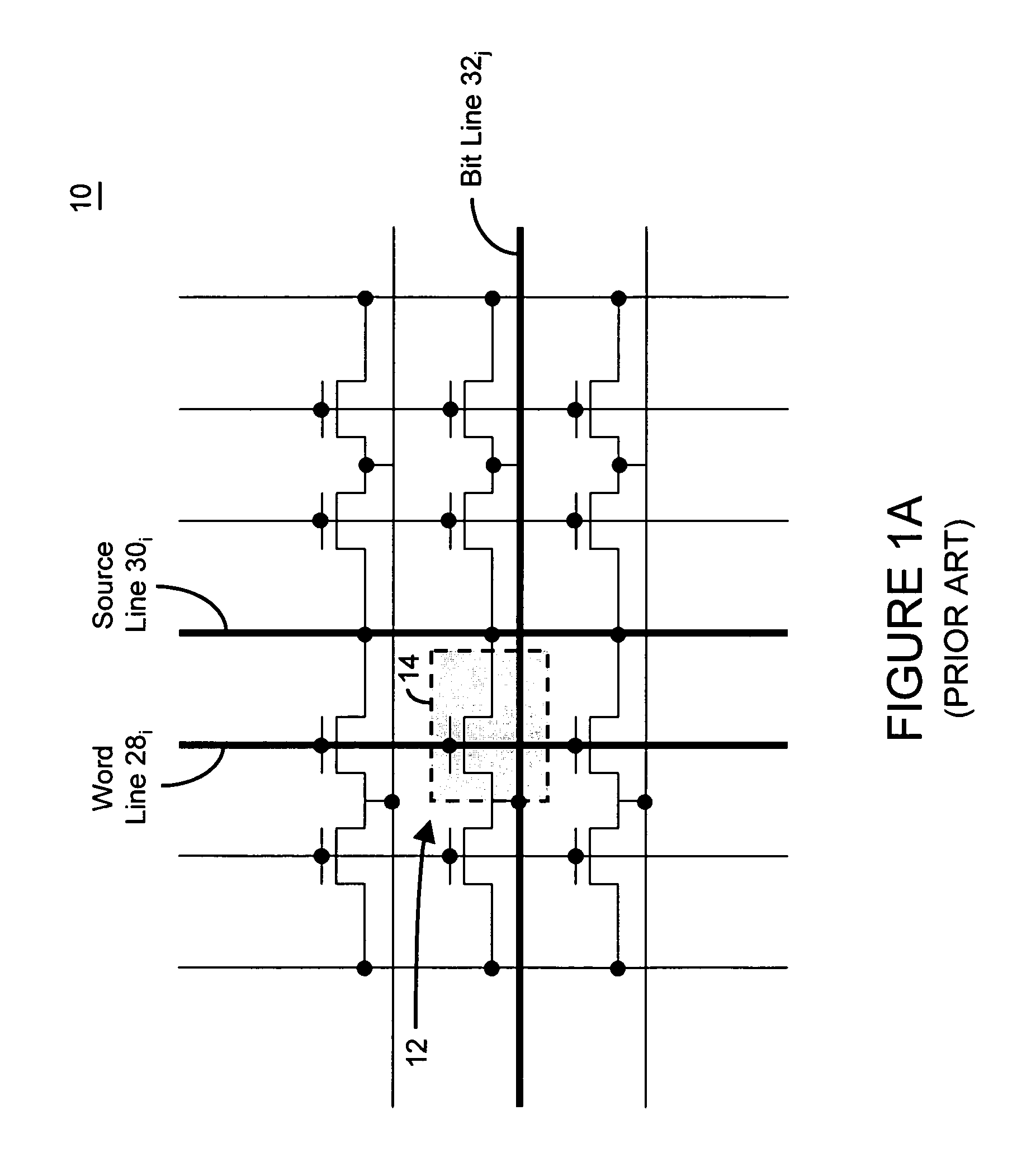
Aside from the consumption of power, writing or programming data into memory cells of an array may also “disturb” adjacent cell memory cells in memory device 10.
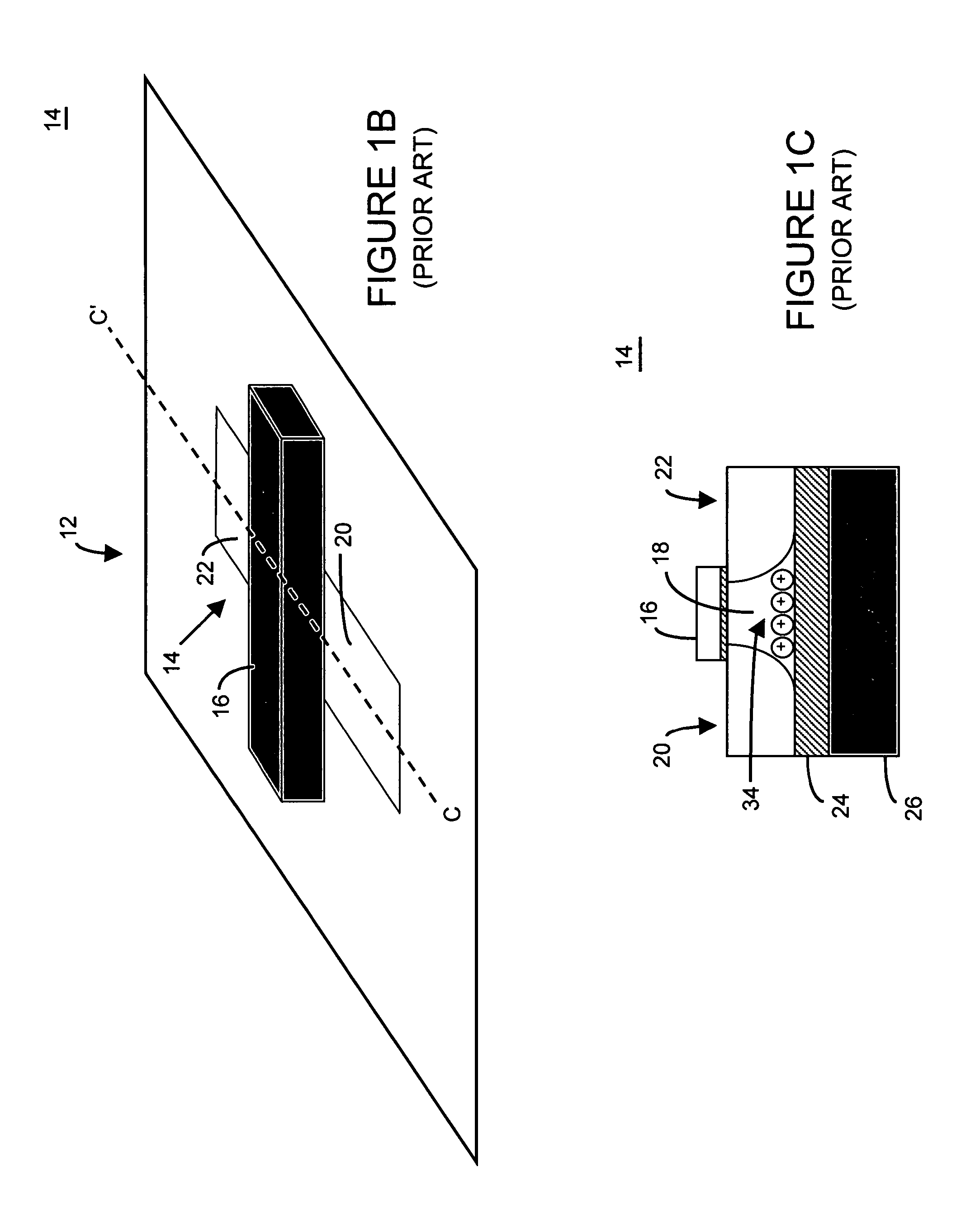
While electrically floating body transistors of memory cells (for example, SOI transistors) of the type described above exhibit low leakage current characteristics, such memory cells often consume a considerable amount of power when programming a logic low (i.e., removing charge carriers from the body of the SOI device).
This may reduce the speed or access time of the memory device, memory array, and / or memory cells.

Method used


Image

  • Memory cell having an electrically floating body transistor and programming technique therefor
  • Memory cell having an electrically floating body transistor and programming technique therefor
  • Memory cell having an electrically floating body transistor and programming technique therefor

Examples


Embodiment Construction

[0042]At the outset, it should be noted that there are many inventions described herein as well as many aspects and embodiments of those inventions.

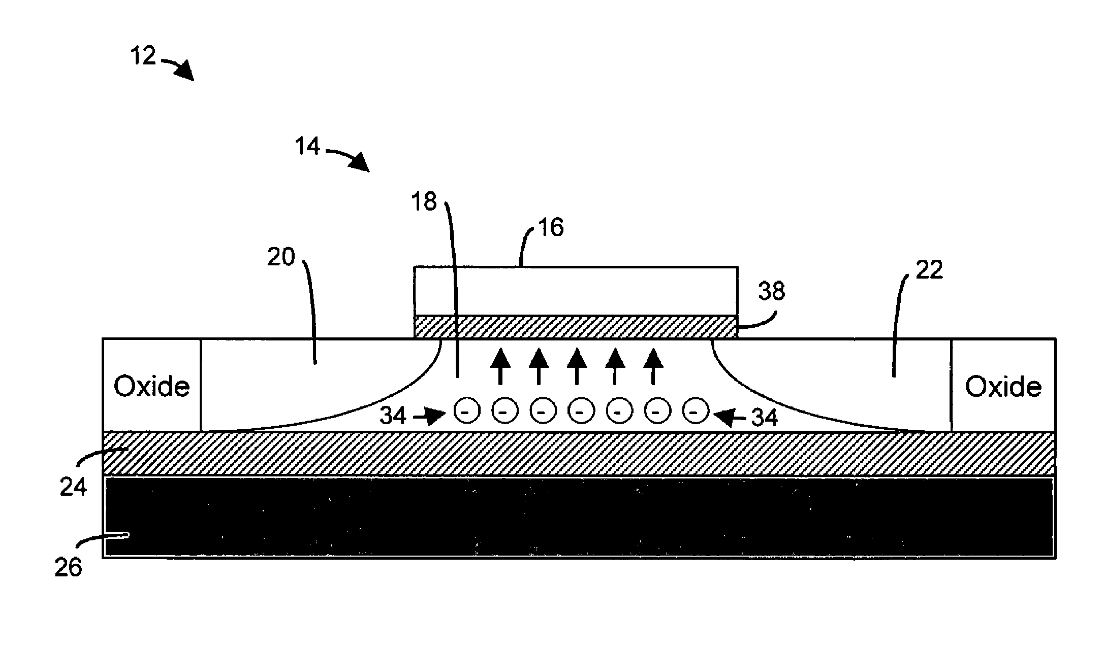
[0043]In a first aspect, the present inventions are directed to a memory cell and / or technique of writing or programming a logic low or State “0” in a memory cell having an electrically floating body transistor. In this regard, in one embodiment, the present inventions program a logic low or State “0” in the memory cell by causing, forcing and / or inducing majority carriers in the floating body to tunnel through or traverse the gate dielectric to the gate of the electrically floating body transistor (and, in many array configurations, the word line in the context of a memory cell array). As such, a carrier concentration, which is representative of a logic low or “0” data state, is provided (or substantially provided) in the electrically floating body by removing majority carriers from the electrically floating body to the gate of the elec...


PUM


Abstract

A memory cell comprising an electrically floating body transistor including a source region, a drain region, a body region disposed therebetween, wherein the body region is electrically floating, and a gate disposed over the body region and separated therefrom by a gate dielectric. The memory cell includes a first data state representative of a first charge in the body region and a second data state representative of a second charge in the body region wherein the second charge is substantially provided by removing carriers from the body region through the gate. Thus, a memory cell may be programmed to a logic low by, for example, causing, forcing and / or inducing carriers in the floating body of the transistor to tunnel through or traverse the gate dielectric to the gate of the electrically floating body transistor (and, in many array configurations, the word line of a memory cell array).

Description

RELATED APPLICATIONS[0001]This application claims priority to U.S. Provisional Application Ser. No. 60 / 625,248, entitled “Programming Technique for a Memory Cell Having an Electrically Floating Body Transistor”, filed Nov. 4, 2004. The contents of this provisional application are incorporated by reference herein in their entirety.BACKGROUND[0002]In one aspect, the inventions relate to a semiconductor memory cell, array, architecture and device, and techniques for controlling and / or operating such cell and device; and more particularly, in one aspect, to a semiconductor dynamic random access memory (“DRAM”) cell, array, architecture and / or device wherein the memory cell includes an electrically floating body in which an electrical charge is stored.[0003]Briefly, by way of background, there is a continuing trend to employ and / or fabricate advanced integrated circuits using techniques, materials and devices that improve performance, reduce leakage current and enhance overall scaling. S...

Claims


Application Information

Patent Timeline
Patent Type & Authority Patents(United States)
IPC IPC(8): H01L27/12
CPCG11C11/404H01L27/108H01L29/7841G11C2211/4016H01L27/1203H01L29/78654H10B12/00
Inventor OKHONIN, SERGUEINAGOGA, MIKHAIL
Owner MICRON TECH INC
Learn More