Fast image simulation for photolithography

a photolithography and image technology, applied in the field of photolithography, can solve the problem that the simulation technique is not perfect, and achieve the effect of reducing false defect reports, facilitating simulation, and increasing the sensitivity of inspection tools

Active Publication Date: 2008-12-30
PETER J FIEKOWSKY
View PDF4 Cites 9 Cited by
  • Summary
  • Abstract
  • Description
  • Claims
  • Application Information

AI Technical Summary

Benefits of technology

[0010]In a second embodiment of the invention useful in practice, several steps are combined. The microscope resolution is typically two to three times higher than the stepper resolution being simulated. This fact allows steps to be combined because deconvolution as a separate step is not required. Thus, the deconvolution step may be eliminated by reducing the amount of blurring used to produce the aerial image. In addition, the dilation and erosion steps used to produce the aerial image are combined into a single erosion.
[0015]The simulated image may then be used to calculate edge position errors, CD errors, feature position errors and contrast errors. Because the simulation occurs much more quickly, these measurements can be used to decrease false defect reports from inspection tools, and to allow for increased sensitivity of inspection tools. A faster simulation also helps to accelerate process development for new products by allowing more variables to be tried, and improves OPC (optical proximity correction) techniques as more adjustments can be tried.

Problems solved by technology

No technique for simulation will be perfect.

Method used


Image

  • Fast image simulation for photolithography
  • Fast image simulation for photolithography
  • Fast image simulation for photolithography

Examples


first simulation embodiment

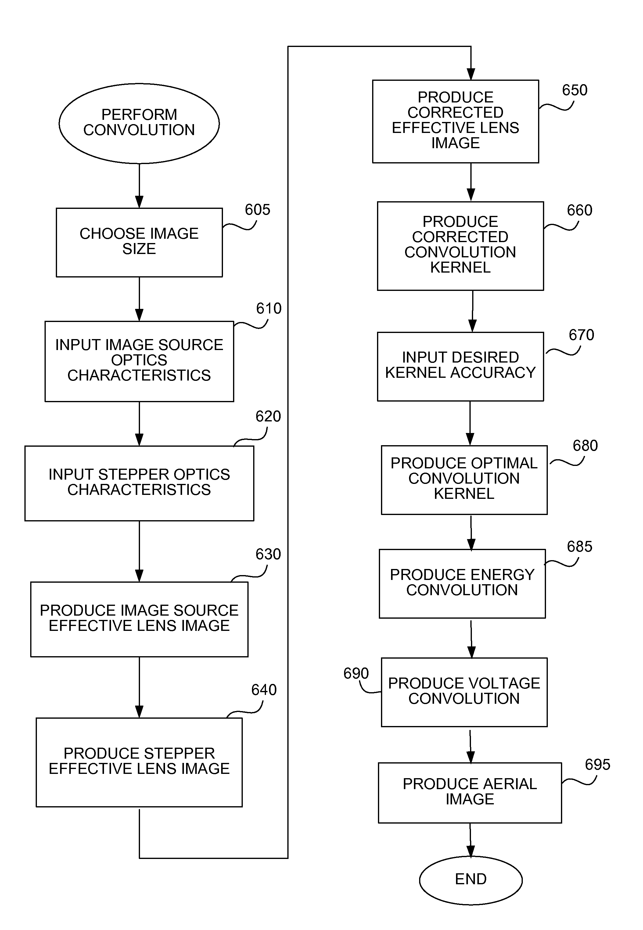
[0034]As pointed out above, the present invention models blurring and edge diffraction to quickly produce an accurate simulation. As is commonly known, an image taken of a photomask (using a typical video inspection machine) having sub-micron dimensions will appear blurred as described above in the Rayleigh criterion by the resolution of the optical system. This blurring is corrected, typically by deconvolution. Images that come directly from the mask design, without optics, will not require this correction.

[0035]Photons that come closer to the edge than Res / 4.4, where Res is the Rayleigh resolution, are diffracted beyond the opening of the objective lens and appear to be blocked by the dark area of the photomask. This diffraction causes dark areas to appear larger at low optical resolution than at high resolution. A dark line, which consists of two edges, is observed to be Res / 2.2 larger than observed with an SEM, and a clear line is observed to be smaller by the same amount. Becau...

second simulation embodiment

[0045]In a second simulation embodiment, optimizations are used to speed up generation of the simulation, by a factor of 2 to 5× faster. For example, as dilation and erosion are sequentially applied to the image after deconvolution, it is possible to combine these two processing steps into a single erosion step. The single step ends up being an erosion (rather than a dilation) because the need to slightly widen lines (to match the stepper resolution) slightly outweighs the need to narrow lines due to edge diffraction in the source image optics. In other words, an erosion is performed, but the amount is reduced because of the dilation required. Or more simply, lines are widened to compensate for the stepper resolution, but not quite so much in order to compensate for the diffraction in the source image.

[0046]Also, because the source image resolution is high compared to the stepper resolution, the deconvolution step is not needed because image 310 is sharper than image 350. Since the ...


PUM


Abstract

A fast method simulates photolithography using conventional image processing techniques. Convolution simulates blurring due to optics; erosion and dilation correct for edge diffraction. To produce the convolution kernel, an effective projection lens image for the image source is produced by convolving the lens image with an image of the illuminator aperture shape. An effective projection lens image for the stepper is produced similarly. The stepper effective lens image is divided by the image source effective lens image to produce a corrected effective lens image. A corrected convolution kernel is produced by taking a Fourier transform of the corrected effective lens image. The kernel is used to convolve the image, once using energy and once using voltage, and then squaring the result. The aerial image is produced by blending the energy and voltage convolutions according to the computed partial coherence of the optics. Complex convolution is used to represent relative phases other than 180 degrees.

Description

FIELD OF THE INVENTION[0001]The present invention relates generally to photolithography. More specifically, the present invention relates to the simulation of an image during semiconductor manufacturing.BACKGROUND OF THE INVENTION[0002]Photolithography is the process of transferring geometric shapes on a photographic mask to the surface of a silicon wafer; it falls under the more broad category of microlithography. A photographic mask (or “photomask”), typically a glass plate with a patterned emulsion of metal film on one side, is used in photolithography to create integrated circuits. Chromium (chrome) is typically used to produce the pattern on the photomask.[0003]The successful manufacture of advanced sub-micron sized semiconductor devices requires accuracy in production of the photomask, and in the photolithography processes used to pattern the wafer. Photolithography processes for semiconductor manufacturing frequently use image simulation for predicting the outcome of the manu...

Claims


Application Information

Patent Timeline
Patent Type & Authority Patents(United States)
IPC IPC(8): G06F17/50
CPCG03F1/144G03F1/36G03F7/705
Inventor FIEKOWSKY, PETER J.SCHUSTER, RICHARD E.
Owner PETER J FIEKOWSKY
Why Eureka
Try Eureka