Thin film transistor array and electrostatic discharge protective device thereof

a thin film transistor and array technology, applied in the field of thin film transistor arrays, can solve the problems of permanently disabling circuitry, damaging circuit devices in integrated circuits and other circuitry, harming lcd devices, etc., and achieve the effect of not being able to detect defective pixels

Inactive Publication Date: 2008-12-30
CHUNGHWA PICTURE TUBES LTD
View PDF7 Cites 7 Cited by
  • Summary
  • Abstract
  • Description
  • Claims
  • Application Information

AI Technical Summary

Benefits of technology

[0008]Accordingly, the present invention is directed to a TFT array and an ESD protective device thereof, which can prevent devices on TFT array from ESD damage, and is impossible to detect a defective pixel.

Problems solved by technology

Electrostatic discharge is a phenomenon that electrostatic charge moves along the surface of a non-conductive material, which might damage circuit devices in an integrated circuit and other circuitry.
During a fabrication process of a liquid crystal display (LCD), relevant machinery platforms and technicians under operation can carry electrostatic charges, thus when these charge bearers contact the LCD panels, an electrostatic discharge event might take place, and the momentary discharge might harm the LCD devices and permanently disable the circuitry.
Conversely, when a voltage is applied to the scan line to thereby read the data of the testing pixel from the data line, the voltage is applied via the common driving signal line to other scan lines, and it is impossible to derive a voltage peculiar to the pixel.
Thus, it is impossible to detect a defective pixel.

Method used


Image

  • Thin film transistor array and electrostatic discharge protective device thereof
  • Thin film transistor array and electrostatic discharge protective device thereof
  • Thin film transistor array and electrostatic discharge protective device thereof

Examples


Embodiment Construction

[0050]Reference will now be made in detail to the present preferred embodiments of the invention, examples of which are illustrated in the accompanying drawings. Wherever possible, the same reference numbers are used in the drawings and the description to refer to the same or like parts.

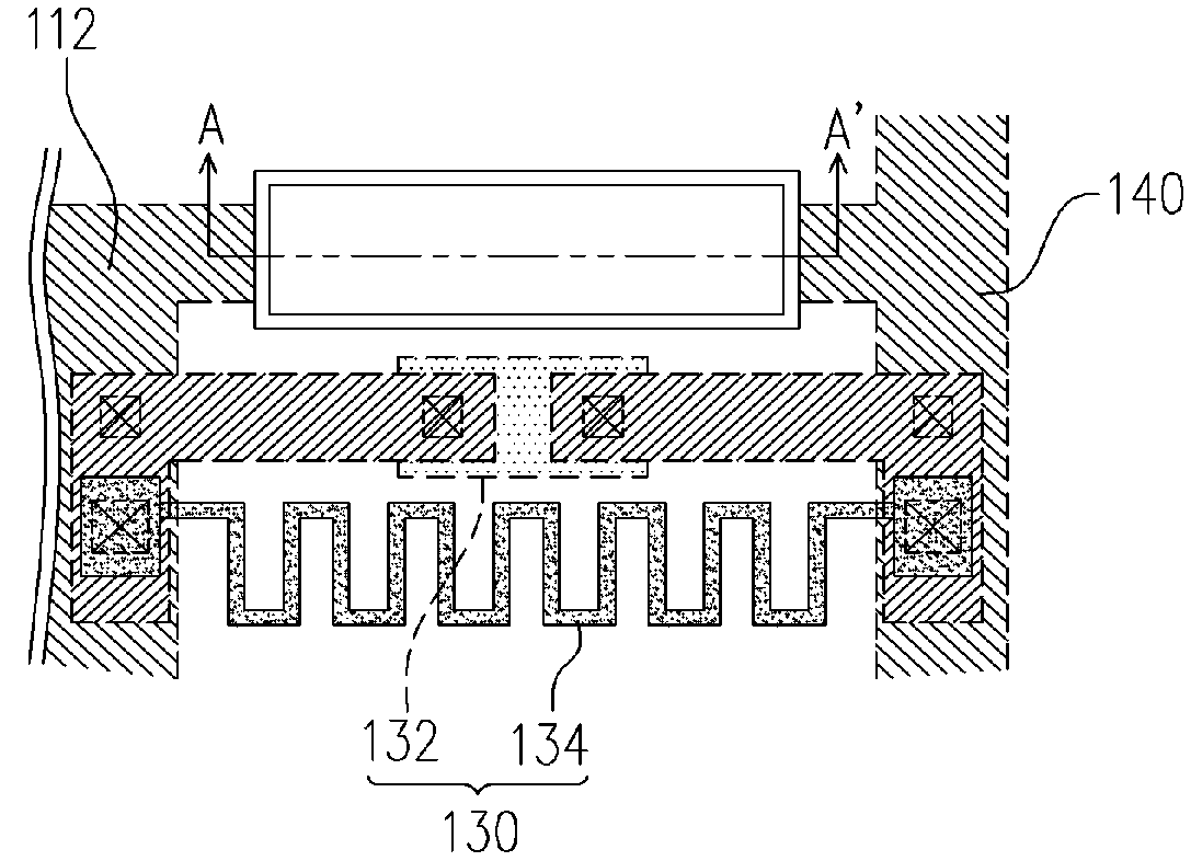
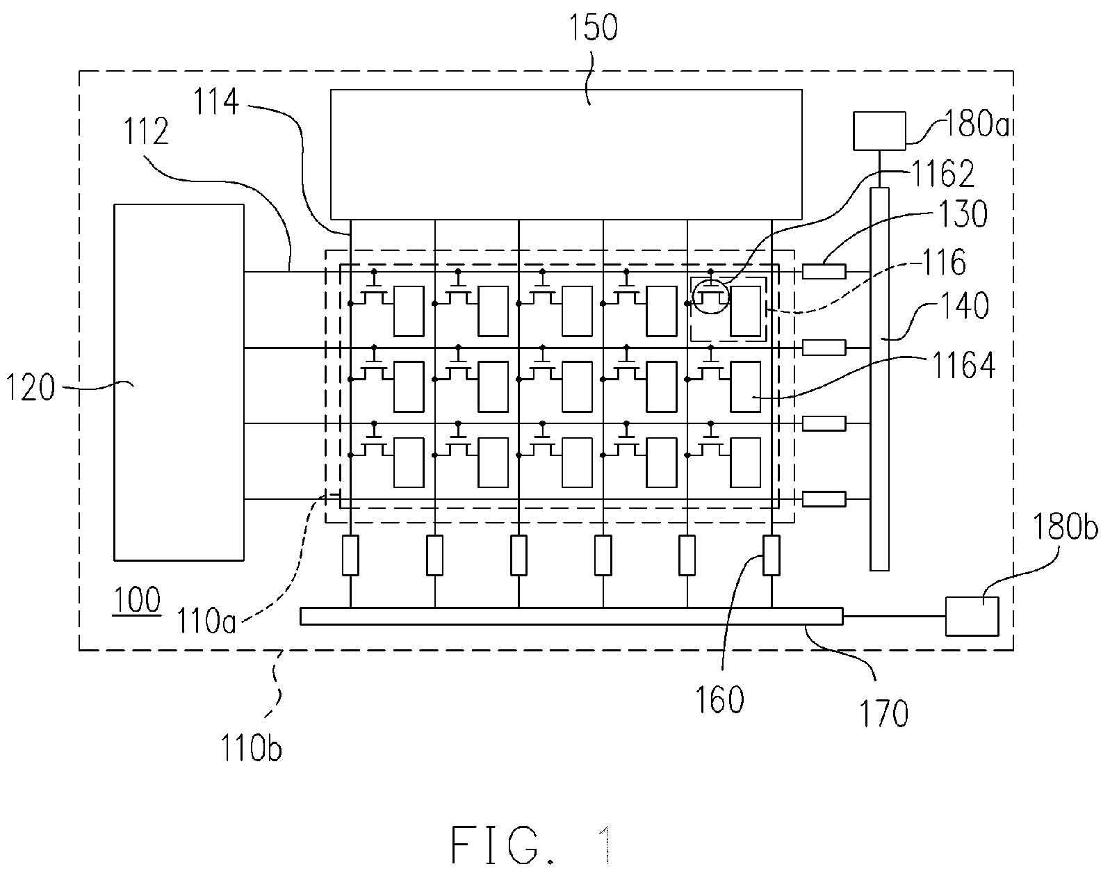
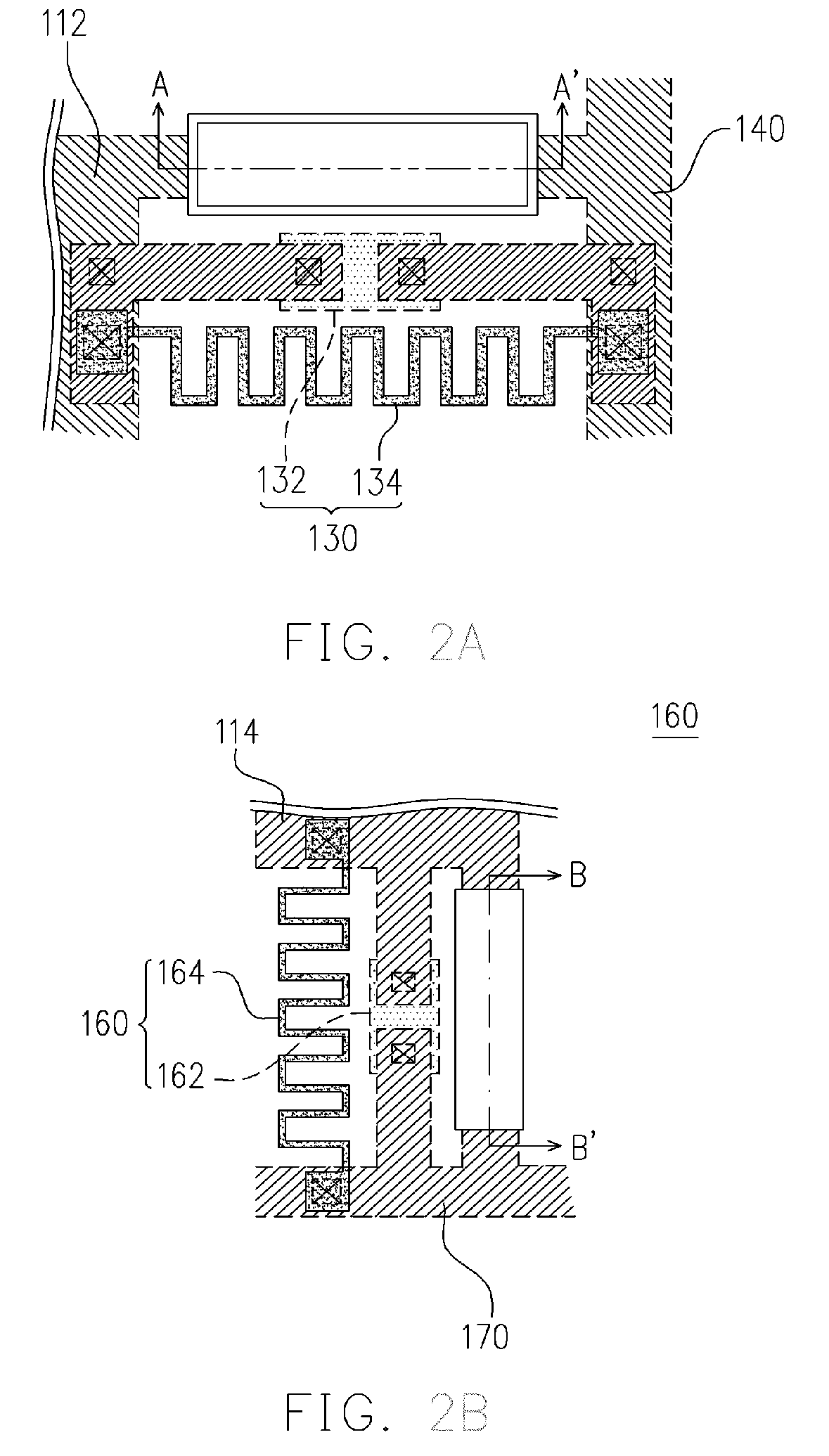
[0051]FIG. 1 is a top view illustrating a TFT array and an ESD protective device thereof according to the present invention. Referring to FIG. 1, the TFT array 100 comprises a substrate (not shown), a plurality of scan lines 112, a plurality of data lines, a plurality of pixel structures, a scan driving circuit 120, a plurality of first ESD protective devices 130, a first shorting bar 140, a data driving circuit 150, a plurality of second ESD protective devices 160, and a second shorting bar 170.

[0052]The substrate has a display region 110a and a peripheral circuit region 110b. Wherein, the display region 110a is used for display image, and related circuits are disposed in the peripheral circuit regi...


PUM


Abstract

A thin film transistor array, an electrostatic discharge protective device thereof, and methods for fabricating the same are provided. The thin film transistor array comprises a plurality of scan lines, a plurality of data lines, a first shorting bar, and a second shorting bar. The electrostatic discharge protective device comprises a switching device and a resistance line in parallel. If static electricity accumulated on the TFT array is over a predetermined range, the accumulated static electricity will be conducted to the first or second shorting bar via the switching device. The resistance line can prevent signals applied to one of the scan lines or data lines from being conducted to other scan lines or data lines, to detect a defective pixel.

Description

BACKGROUND OF THE INVENTION[0001]1. Field of the Invention[0002]The present invention generally relates to a thin film transistor (TFT) array and a fabricating method thereof. More particularly, the present invention relates to a top-gate TFT array, an ESD protective device thereof, and methods for fabricating the same.[0003]2. Description of Related Art[0004]Electrostatic discharge is a phenomenon that electrostatic charge moves along the surface of a non-conductive material, which might damage circuit devices in an integrated circuit and other circuitry. For instance, when a human being is walking on a carpet, hundreds or even thousands of voltages of electrostatic potential might be detected under high relative humidity, whereas even tens of thousands of voltages might be detected under low relative humidity.[0005]During a fabrication process of a liquid crystal display (LCD), relevant machinery platforms and technicians under operation can carry electrostatic charges, thus when ...

Claims


Application Information

Patent Timeline
Patent Type & Authority Patents(United States)
IPC IPC(8): H01L27/148H01L23/62H01L29/04H01L29/768H01L31/036
CPCH01L27/0251H01L27/12H01L27/1248H01L27/124H01L29/78675
Inventor CHEN, CHEN-MING
Owner CHUNGHWA PICTURE TUBES LTD
Why Eureka
Try Eureka