
Method for inspecting insulating film for film carrier tape for mounting electronic components thereon, inspection apparatus for inspecting the insulating film, punching apparatus for punching the insulating film, and method for controlling the punching apparatus

a technology of electronic components and inspection methods, applied in the direction of individual semiconductor device testing, semiconductor/solid-state device testing/measurement, instruments, etc., can solve problems such as fins, defects such as dents remaining in the subsequent step, and products for clients, so as to improve production yield and avoid inspection failures of operators , the effect of variable inspection accuracy

Inactive Publication Date: 2008-08-05
MITSUI MINING & SMELTING CO LTD
View PDF16 Cites 2 Cited by
  • Summary
  • Abstract
  • Description
  • Claims
  • Application Information

AI Technical Summary

Benefits of technology

The present invention provides a method and apparatus for inspecting and punching an insulating film for film carrier tape. The method involves irradiating the insulating film with parallel rays and detecting defects through image processing. The apparatus includes a conveying system, a light source, a polarizing filter, an image pickup device, and an inspecting means. The technical effects of the invention include reducing defects on the film surface caused by punching, reducing the number of pieces with defects, and minimizing the impact of debris on the insulating film.

Problems solved by technology

Therefore, after punching of a conveyed insulating film for film carrier tape, operators visually find defects such as dents and fins through observation under a microscope.
Since the inspection is carried out visually, inspection accuracy has varied among the operators, and some operators have failed to find such defects.
Thus, in some cases, defects such as dents remain in a subsequent step and, furthermore, in the products for clients.
However, when a punched insulating film for film carrier tape is dented due to debris from being lifted or similar abnormality in a punching mold during production thereof or when an insulating film for film carrier tape is dented due to a foreign matter attached on the film per se, a lot of failure pieces are not detected and must be discarded, thereby lowering production yield with respect to the starting material.

Method used


Image

  • Method for inspecting insulating film for film carrier tape for mounting electronic components thereon, inspection apparatus for inspecting the insulating film, punching apparatus for punching the insulating film, and method for controlling the punching apparatus
  • Method for inspecting insulating film for film carrier tape for mounting electronic components thereon, inspection apparatus for inspecting the insulating film, punching apparatus for punching the insulating film, and method for controlling the punching apparatus
  • Method for inspecting insulating film for film carrier tape for mounting electronic components thereon, inspection apparatus for inspecting the insulating film, punching apparatus for punching the insulating film, and method for controlling the punching apparatus

Examples


Embodiment Construction

[0049]With reference to the attached drawings, preferred embodiments of the method for inspecting an insulating film for film carrier tape, the inspection apparatus, the punching apparatus for punching an insulating film for film carrier tape, and the method for controlling the punching apparatus according to the present invention will next be described in detail.

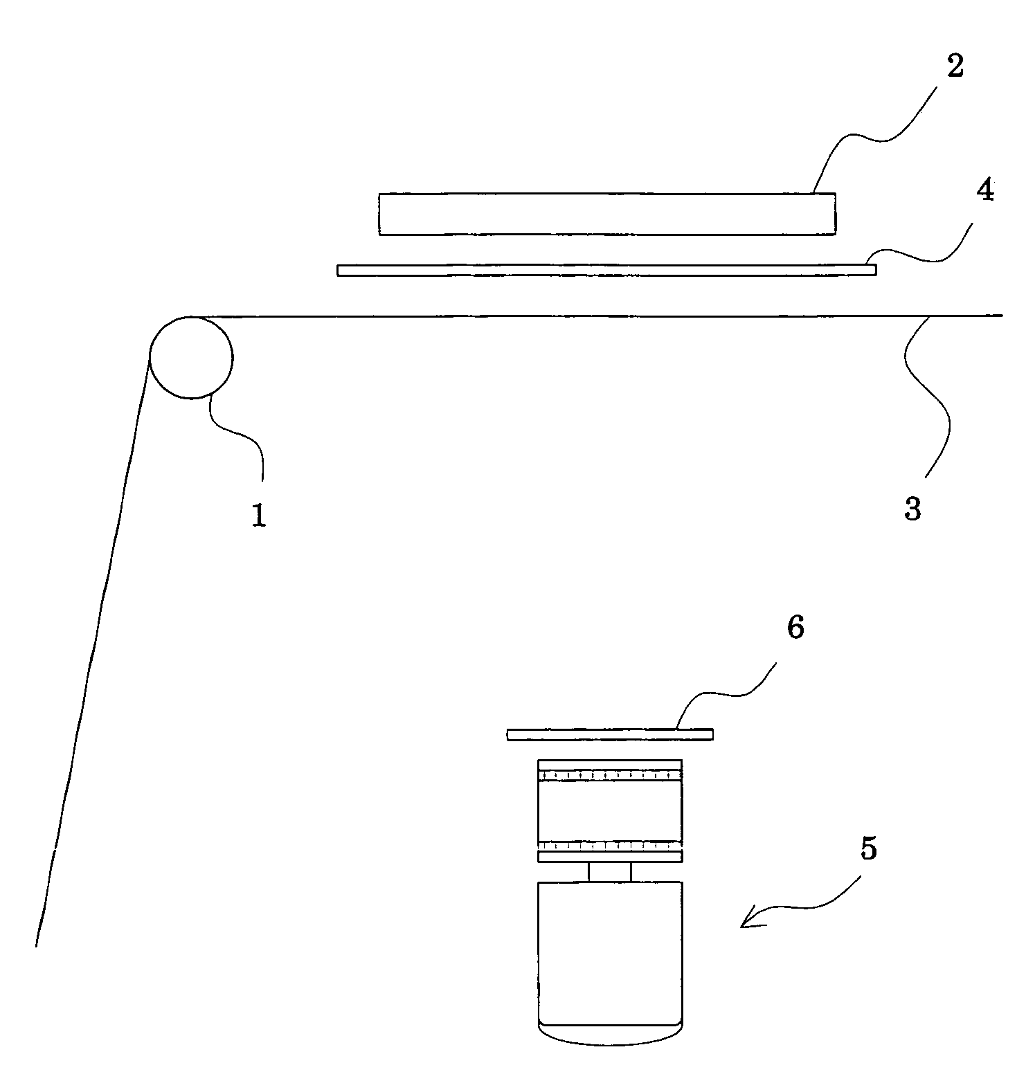
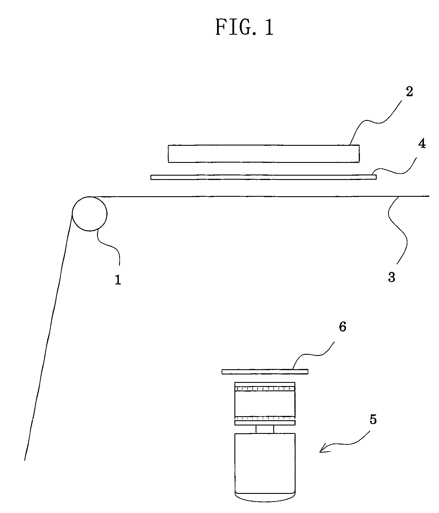
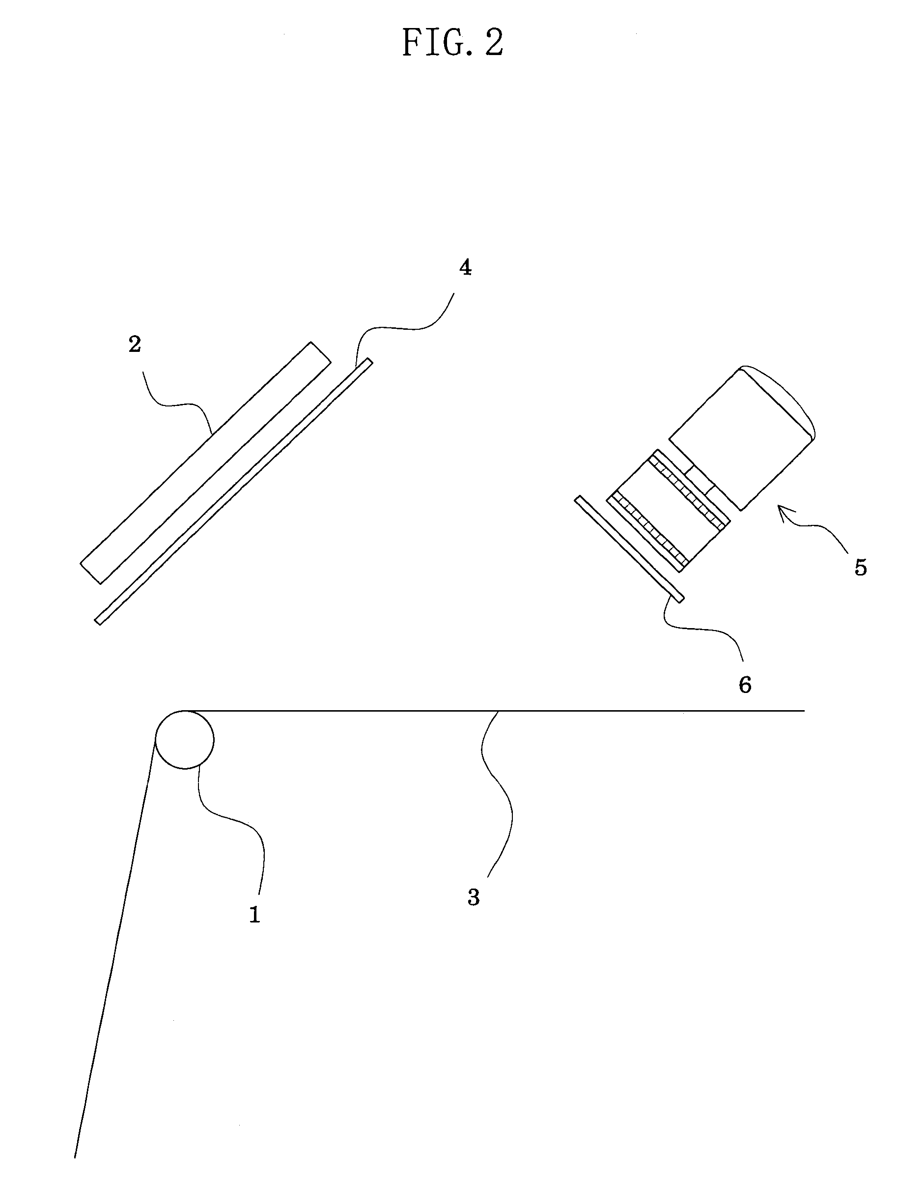
[0050]FIG. 1 shows an inspection apparatus for detecting defects present inside or on the top surface or the bottom surface of an insulating film 3 for film carrier tape, the apparatus comprising: a conveying means 1 (e.g. a roller) for conveying the insulating film 3 for film carrier tape; a light source 2 (e.g., an LED) for emitting parallel rays; a first polarizing filter 4 disposed between the light source 2 and a conveying path for the insulating film 3 for film carrier tape; an image pickup device 5 (e.g., a CCD camera); a second polarizing filter 6 disposed between the image pickup device 5 and the conveying path for...


PUM

PropertyMeasurementUnit
insulatingaaaaaaaaaa
brightnessaaaaaaaaaa
areasaaaaaaaaaa

Abstract

The invention provides an inspection apparatus and an inspection method for detecting defects, a punching apparatus, and a method for controlling a punching apparatus, for the purpose of immediate detection of debris from being lifted toward the surface of an insulating film for film carrier tape, which debris tends to occur during punching of the insulating film for film carrier tape by use of a punching mold, whereby the number of pieces having defects on the film surface caused by attachment of debris from being lifted or foreign matter is reduced to a minimum possible number. In the present invention, an insulating film for film carrier tape is irradiated with parallel rays having passed through a first polarizing filter, the insulating film having been punched and being conveyed; the rays having passed through or having been reflected by the insulating film for film carrier tape is caused to pass through a second polarizing filter; the rays having passed through the second polarizing filter, is received by means of an image pickup device; and the image input to the image pickup device is subjected to image processing as a difference of brightness, whereby defects of the insulating film for film carrier tape are detected.

Description

BACKGROUND OF THE INVENTION[0001]1. Field of the Invention[0002]The present invention relates to a method for inspecting insulating film (in the form of a long tape or sheet) for use in production of a film carrier tape for mounting electronic components thereon, such as a TAB (tape automated bonding) tape, a COF (chip on film) tape, a CSP (chip size package) tape, a BGA (ball grid array) tape, a μ-BGA (μ-ball grid array) tape, a FC (flip chip) tape, a QFP (quad flat package) tape, or an FPC (flexible printed circuit) tape (hereinafter such tapes are collectively referred to simply as film carrier tapes); to an inspection apparatus for detecting defects of an insulating film for film carrier tape for mounting electronic components thereon (hereinafter referred to simply as “an insulating film for film carrier tape ”); to a punching apparatus for punching an insulating film for film carrier tape; and to a method for controlling a punching apparatus for punching an insulating film for...

Claims


Application Information

Patent Timeline
Patent Type & Authority Patents(United States)
IPC IPC(8): G01R31/26H01L21/66G01N21/00G01B11/30G01N21/21G01N21/89G01N21/892
CPCG01N21/8901G01N21/21A01K93/00A01K95/02
Inventor KATO, KAZUYOSHIHORIAI, NAOAKI
Owner MITSUI MINING & SMELTING CO LTD
Learn More