Methods and apparatus for measuring morphology of a conductive film on a substrate

a technology of conductive film and substrate, applied in the direction of electrical/magnetic thickness measurement, material magnetic variables, instruments, etc., can solve the problems of destroying one or more substrates, affecting the morphology of affecting the morphology of the conductive film on the substrate, etc., and affecting the morphology of the substrate. , to achieve the effect of reducing the time required for plasma processing, reducing the cost of processing, and reducing the cost a technology of a a technology of a a technology of a a technology of a a a technology of a a a a a a a a technology of a a a a a a a a a a technology of a a a a a a a technology of a substrate morphology, applied in the field, can solve the problem of the substrate morphology analysis, the substrate morphology analysis

Inactive Publication Date: 2008-07-22
LAM RES CORP
View PDF9 Cites 10 Cited by
  • Summary
  • Abstract
  • Description
  • Claims
  • Application Information

AI Technical Summary

Problems solved by technology

For example, if a process involves multiple steps, each with its own gas mixture, gas pressure, RF voltage and power settings, and duration, it is difficult to ascertain exactly, by examining a post-process substrate, which parameter in which step did not conform to specifications and is thus likely to be the source of the defects.
In metrology, one can refer back to the log file to obtain more information but the process is not integrated and requires one or more substrate runs (and possibly ruining one or more substrates) before the problem is spotted.
Furthermore, the whole cycle of processing a substrate, examining the processed substrate, and troubleshooting the plasma processing system based on the data obtained from the processed substrates may take a substantial amount of time.
If multiple cycles are required to remedy a manufacturing, installation, or qualification problem, the multiple cycle times increase the total time and effort required to bring a plasma processing system on line for production, thereby contributing to a higher cost of ownership even before a single production IC is created.
While equipment manufacturers try to create a maintenance schedule that cleans and / or replaces parts before problems arise, equipment failure would still occur sometimes. Since raw substrates, processed gases, and plasma processing systems are all expensive, IC manufacturers are motivated to detect failures as quickly as possible to minimize further damage to substrates and / or other subsystems of the plasma processing system and to remedy the failure found to bring the plasma processing system back on line quickly.
Again, while the processed substrates can furnish certain data useful in monitoring the production of ICs in installed and / or upgraded plasma processing systems, there are disadvantages associated with relying primarily on substrates data to guide the operation and / or maintenance of the plasma processing system.
As discussed in the earlier example, if a process involves multiple steps, each with its own gas mixture, gas pressures, RF voltages and power settings, and duration, it is difficult to ascertain exactly, by examining a post-process substrate, which parameter in which step did not conform to specifications and is thus likely to be the source of the defects.
Furthermore, the whole cycle of processing a substrate, examining the processed substrate, and troubleshooting the plasma processing system based on the data obtained from the processed substrates may take a substantial amount of time.
If multiple cycles are required, the multiple cycle times increase the total time and effort required to remedy the failure and to bring the plasma processing system back on line for production use, thereby contributing to a higher average cost per substrate successfully processed.
Likewise, a lower temperature generally increases conductivity, and hence the resulting the eddy current response, while a higher temperature generally reduces conductivity, and hence the resulting eddy current response as well.
If this first field is brought into proximity with a second conductor (e.g., a conductive layer on the substrate) a second alternating electrical current will also flow in the second conductor, causing a second field that interacts with (e.g., adds vectorally to) the first field and results in a perturbation to the field around the probe.
These perturbations in the probe's initial field may cause detectable changes in the probe's electrical characteristics including the probe's impedance and frequency response.
However, the electrical response of sensor to the magnetic field (eddy current perturbations), and hence its accuracy, may also be affected by the proximity (substrate proximity response) of the sensor to the substrate.
In general, it is difficult to isolate the portion of the electrical response caused by electrical film properties (electrical film property response) from the portion of the electrical response caused by proximity (substrate proximity response), which may subsequently introduce an error in the reported value.
However, common methods of eddy current measurement presume the lack of edge effects to create eddy current discontinuities.
That is, the smaller the coil or magnetic sheathing at the tip, the more spatially restricted and hence the more spatially sensitive (and expensive) the eddy current sensor.
Subsequently, reducing the size of the coil would only reduce the discontinuity effect of the substrate edge, and not eliminate it.
Additional problems with sensor system repeatability and complexity may plague a solution attempting to reduce the edge effect by reducing the spatial size of the eddy current inducing field region.
However, this method tends to be sensitive to the data input.
Subsequently, many more measurements may be required to achieve a sufficient level of accuracy, substantially slowing down the measuring process.

Method used


Image

  • Methods and apparatus for measuring morphology of a conductive film on a substrate
  • Methods and apparatus for measuring morphology of a conductive film on a substrate
  • Methods and apparatus for measuring morphology of a conductive film on a substrate

Examples


Embodiment Construction

[0035]The present invention will now be described in detail with reference to a few preferred embodiments thereof as illustrated in the accompanying drawings. In the following description, numerous specific details are set forth in order to provide a thorough understanding of the present invention. It will be apparent, however, to one skilled in the art, that the present invention may be practiced without some or all of these specific details. In other instances, well known process steps and / or structures have not been described in detail in order to not unnecessarily obscure the present invention.

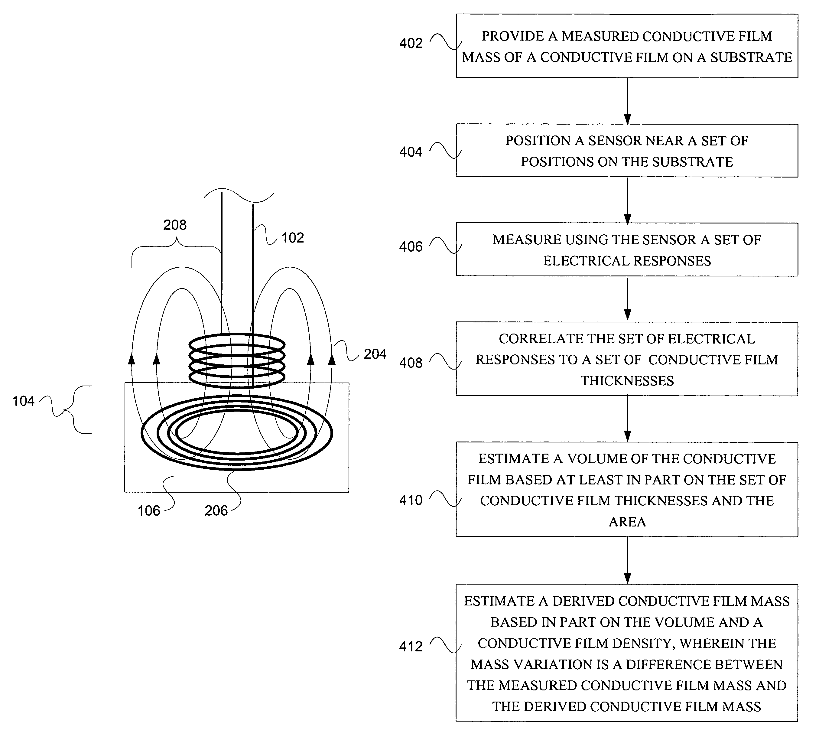
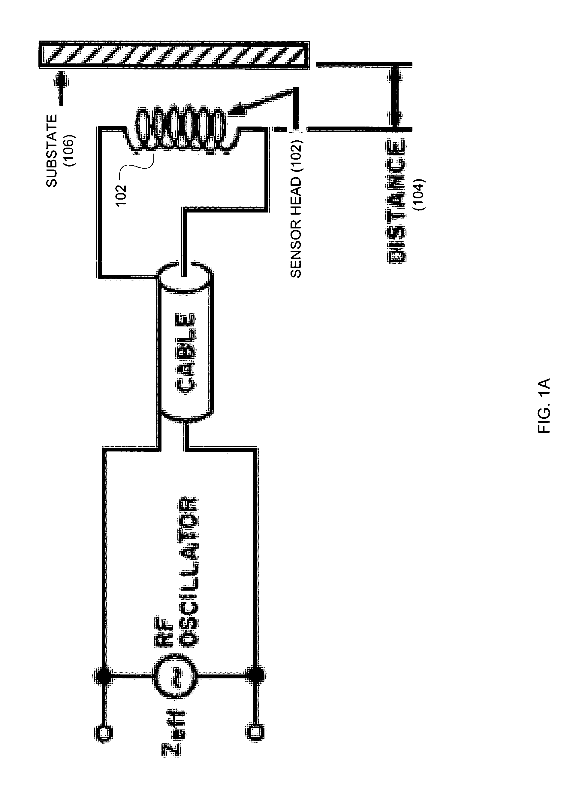
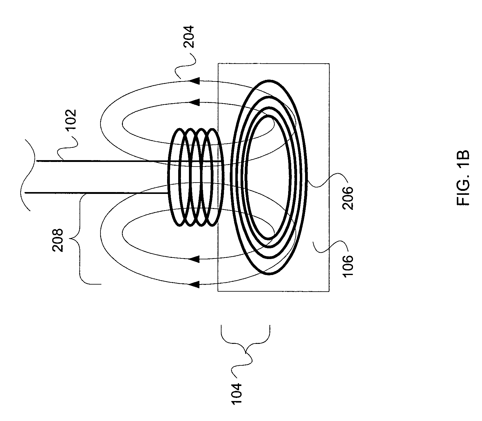
[0036]While not wishing to be bound by theory, it is believed by the inventor herein that the morphology (i.e., texture, topography, etc.) of a conductive film on a substrate may be measured through the use of eddy currents. That is, eddy current conductivity correlation may be confounded with film thickness variation at particular thickness positions on the substrate, in order to determin...


PUM

PropertyMeasurementUnit
thicknessaaaaaaaaaa
conductiveaaaaaaaaaa
massaaaaaaaaaa

Abstract

A method of determining a mass variation of a conductive film on a substrate with an area, an edge zone, and a center zone, is disclosed. The method includes providing a measured conductive film mass of a conductive film on a substrate. The method also includes positioning a sensor near a set of positions on the substrate; measuring using the sensor a set of electrical responses; and correlating the set of electrical responses to a set of conductive film thicknesses. The method further includes estimating a volume of the conductive film based at least in part on the set of conductive film thicknesses and the area; and estimating a derived conductive film mass based in part on the volume and a conductive film density, wherein the mass variation is a difference between the measured conductive film mass and the derived conductive film mass.

Description

BACKGROUND OF THE INVENTION[0001]The present invention relates in general to substrate manufacturing technologies and in particular to methods and apparatus for measuring morphology of a conductive film on a substrate.[0002]In the processing of a substrate, e.g., a semiconductor wafer, MEMS device, or a glass panel such as one used in flat panel display manufacturing, plasma is often employed. As part of the processing of a substrate (chemical vapor deposition, plasma enhanced chemical vapor deposition, physical vapor deposition, etc.) for example, the substrate is divided into a plurality of dies, or rectangular areas, each of which will become an integrated circuit. The substrate is then processed in a series of steps in which materials are selectively removed (etching) and deposited (deposition) in order to form electrical components thereon.[0003]Metals are particularly important materials in substrate manufacturing. For example, in a manufacturing method, known as dual damascen...

Claims


Application Information

Patent Timeline
Patent Type & Authority Patents(United States)
IPC IPC(8): G01N27/72G01B7/06G01R33/12G01R33/14
CPCG01B7/105G01R33/14G01N27/90
Inventor BAILEY, III, ANDREW D.
Owner LAM RES CORP
Why Eureka
Try Eureka