
Digital phase locked circuit capable of dealing with input clock signal provided in burst fashion

Inactive Publication Date: 2008-07-08
FUJITSU LTD
View PDF8 Cites 3 Cited by
  • Summary
  • Abstract
  • Description
  • Claims
  • Application Information

AI Technical Summary

Benefits of technology

[0019]It is a general object of the present invention to provide a digital phase locked circuit in which the above-mentioned problems are eliminated.
[0020]A more specific object of the present invention is to provide a digital phase locked circuit that can lock a phase of a clock signal supplied in a burst fashion so that a desired characteristic can be satisfied.
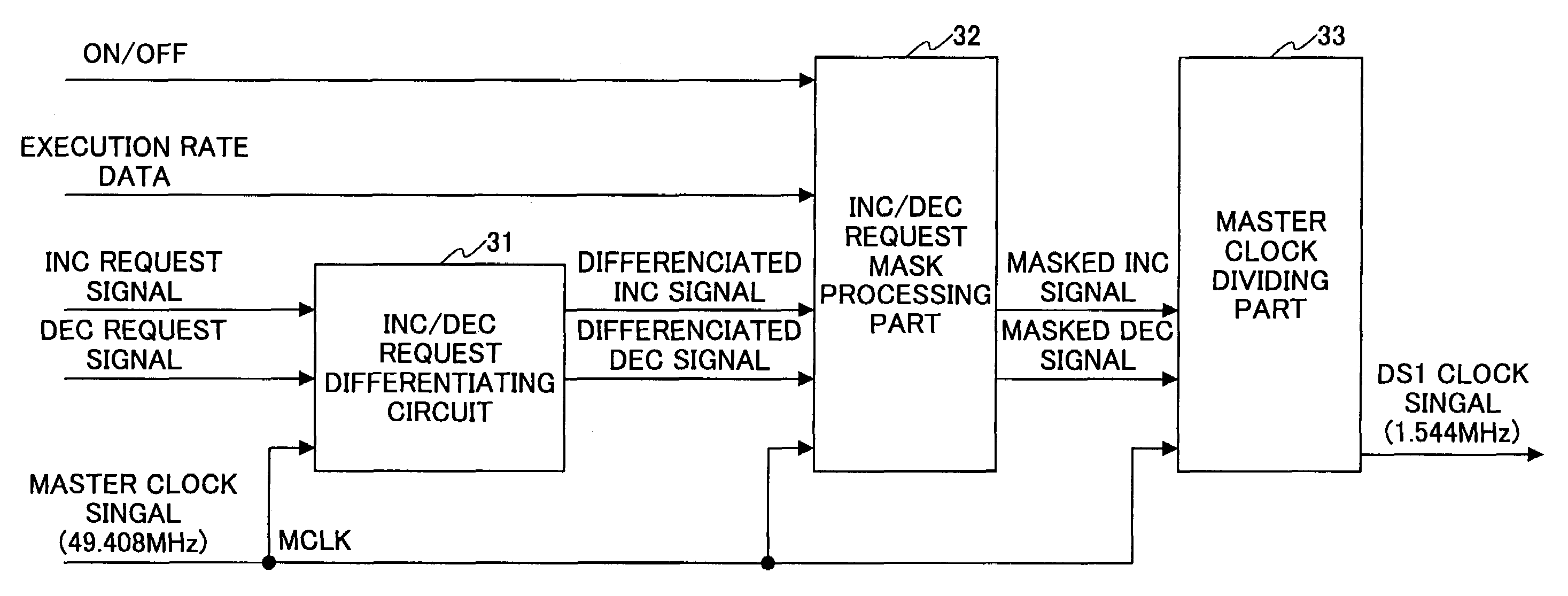
[0026]According to the above-mentioned invention, if the phase difference is large, the digital phase locked circuit increases the execution rate and exhibits high-speed phase absorption characteristics. In contrast, if the phase difference is small, the digital phase locked circuit decreases the execution rate and suppresses jitter. Furthermore, while the phase difference is shifting from a large difference to a small difference, the digital phase locked circuit can set the execution rate so that a desired phase absorption characteristics can be satisfied. As a result, it is possible to obtain an output clock signal phase-synchronous with an input clock signal even if the input clock signal is provided in a burst fashion.

Problems solved by technology

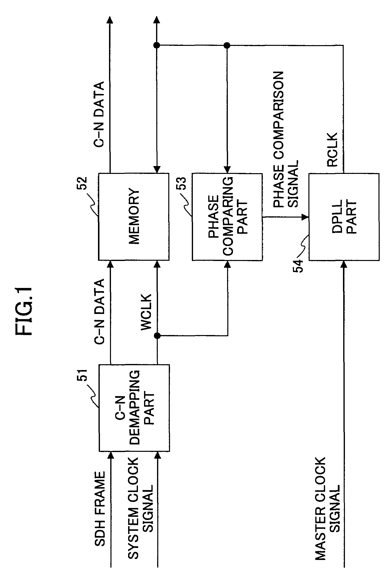
However, when the DPLL circuit is used to process C-N data demapped from a payload of an SDH frame, there arise some problems.
However, since the plurality of the shift registers are provided in the DPLL circuit, the DPLL circuit becomes large in size.
In addition, the DPLL circuit has difficulty in following phase variations of the input data.
In other words, the DPLL circuit cannot achieve the satisfactory phase synchronization characteristic.

Method used


Image

  • Digital phase locked circuit capable of dealing with input clock signal provided in burst fashion
  • Digital phase locked circuit capable of dealing with input clock signal provided in burst fashion
  • Digital phase locked circuit capable of dealing with input clock signal provided in burst fashion

Examples


Embodiment Construction

[0039]In the following, an embodiment of the present invention will be described with reference to the accompanying drawings.

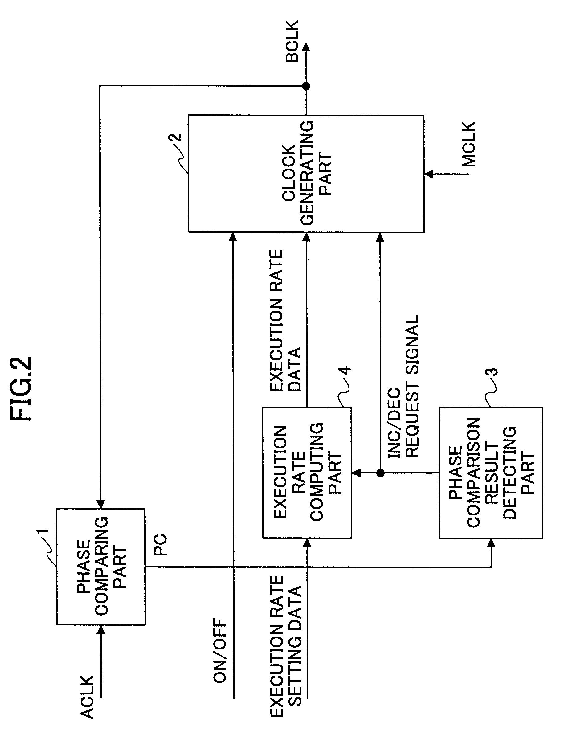
[0040]FIG. 2 shows the structure of a DPLL circuit according to the embodiment of the present invention. As is shown in FIG. 2, the DPLL circuit comprises a phase comparing part 1, a clock generating part 2, a phase comparison result detecting part 3, and an execution rate computing part 4. Also, the DPLL circuit processes a master clock signal MCLK, an input clock signal ACLK, an output clock signal BCLK, a phase comparison signal PC, and a signal ON / OFF for a phase absorption operation.

[0041]The phase comparing part 1 compares the phase of the input clock signal ACLK with the phase of the output clock signal BCLK and then supplies the comparison result signal PC to the phase comparison result detecting part 3. For instance, if it is supposed that the phase comparison result signal PC is generated as an exclusive OR signal of the input clock signal ACLK and t...


PUM


Abstract

A digital phase locked circuit provides an output clock signal whose phase is synchronous with the phase of an input clock signal under a desired level of a phase absorption characteristic even if the input clock signal is supplied in a burst fashion. A phase comparing part compares the phase of the output clock signal with the phase of the input clock signal. A phase comparison result detecting part outputs an INC / DEC request signal for controlling a division operation based on a phase comparison signal. An execution rate computing part computes a phase difference between the input clock signal and the output clock signal based on the INC / DEC request signal and outputs an execution rate corresponding to the phase difference. A clock generating part controls a division operation for the master clock signal in accordance with the INC / DEC request signal and changes phase absorption speed of the output clock signal in accordance with the execution rate.

Description

CROSS-REFERENCE TO RELATED APPLICATIONS[0001]The present application is based on Japanese priority application No. 2002-284761 filed Sep. 30, 2002, the entire contents of which are hereby incorporated by reference.BACKGROUND OF THE INVENTION[0002]1. Field of the Invention[0003]The present invention generally relates to a digital phase locked circuit that can not only output a phase locked signal for an input clock signal even if the input clock signal is supplied in a burst fashion but also achieve a satisfactory phase absorption characteristic.[0004]2. Description of the Related Art[0005]In SDH (Synchronous Digital Hierarchy), STM (Synchronous Transport Module)-1 (155 Mbps) is provided as a fundamental frame. In addition, for instance, STM-0, STM-4 and STM-16 are provided as frames for the bit rates 51 Mbps, 622 Mbps and 2.4 Gbps, respectively.[0006]In the SDH and the similar method, SONET (Synchronous Optical Network), a frame comprises an overhead and a payload. For instance, a c...

Claims


Application Information

Patent Timeline
IPC IPC(8): H03D3/24H03L7/06H03L7/099H03L7/107H04L7/033
CPCH03L7/0993H03L7/107H04J3/076H03L7/1077
Inventor YOKOKURA, ICHIROOBANA, YUJIMOCHIZUKI, HIDEAKI
Owner FUJITSU LTD
Learn More