
Organic light-emitting device and method of fabricating the same

a light-emitting device and organic technology, applied in thermoelectric devices, basic electric elements, electric apparatus, etc., can solve the problems of significant constraints on the use of shadow masks, low light-emitting efficiency, and inability to achieve high resolution, etc., to achieve improved performance and stability, easy control, and desired electrical properties

Inactive Publication Date: 2008-07-01
CAMBRIDGE DISPLAY TECH LTD
View PDF33 Cites 1 Cited by
  • Summary
  • Abstract
  • Description
  • Claims
  • Application Information

AI Technical Summary

Benefits of technology

[0043]The provision of a continuous barrier layer establishes a well defined interface between the upper electrode and the organic layer. The interface between the upper electrode and the organic layer can be controlled by various processes, for example dry or wet cleaning, to which the barrier layer is much more resistant than the organic layer. In the case where inorganic materials such as the above-mentioned metal oxides are used as the barrier layer, the barrier layer acts as a very efficient etch-stop. Edge effects at the edges of pixels, which could occur when a patterned electrode is directly in contact with the adjacent organic layer, are also reduced if not eliminated with the introduction of a continuous barrier layer.
[0044]Such methods of fabricating organic light-emitting devices provide devices of improved performance and stability when the upper electrode deposited over the organic layer is a patterned layer. Preferably, the organic layer is deposited by way of evaporation (resistive or electron-beam) or sputtering (reactive or non-reactive). The preferred method, for example in the case where an inorganic metal oxide is used, is DC magnetron sputtering from a metal or alloy target in the presence of oxygen such that the stoichiometry can be readily controlled and the desired electrical properties can be achieved. RF sputtering from a dielectric target is also a possibility.

Problems solved by technology

High resolution is readily achieved and is principally limited only by the overlap area of the cathode and the anode and thus by the size of the cathode and the anode.
However, shadow masking may not be desirable for various reasons.
In particular, there are significant constraints on the use of shadow masks when displays of large area and / or high resolution are required.
Maintaining the desired electrical and light output characteristics of the pixels in an OLED display when lithographic processes are used to fabricate the electrode patterns, in particular where those patterns are on top of the at least one organic layer, is not trivial owing to the risk of the lithographic processes modifying and potentially damaging the organic layer / electrode interfaces and the vicinity.
Such damage during lithography may originate from the photoresists, the developers, the etching processes (both dry and wet, negative and positive techniques and etch and lift-off) or the solvents used.
Organic electroluminescent and charge transporting materials would normally be damaged, modified and / or etched very rapidly in such dry etching / ashing processes if directly exposed to the plasma.

Method used


Image

  • Organic light-emitting device and method of fabricating the same
  • Organic light-emitting device and method of fabricating the same
  • Organic light-emitting device and method of fabricating the same

Examples


Embodiment Construction

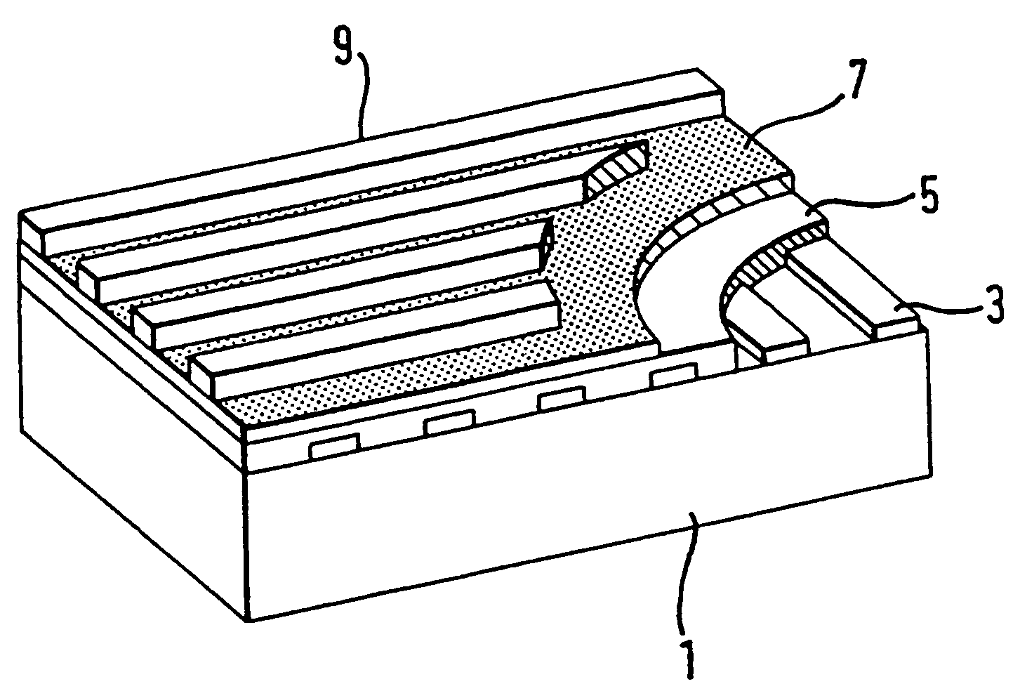
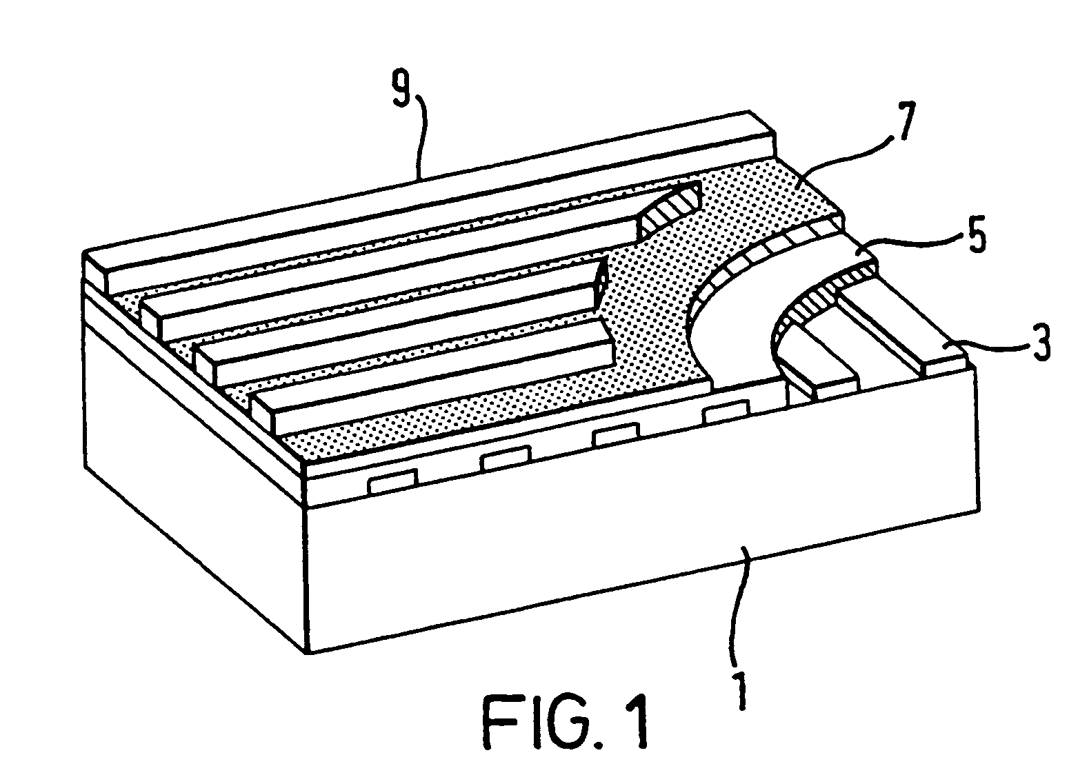
[0049]The organic light-emitting device comprises a substrate 1, an anode 3 formed over the substrate 1, a layer 5 of a light-emissive organic material formed over the anode 3, a barrier layer 7 formed over the organic layer 5, and a cathode 9 formed over the barrier layer 7.

[0050]The substrate 1 is a piece of glass, preferably having a thickness of less than 1.1 mm. The anode 3 is a patterned array of lines, preferably of indium-tin oxide having a thickness of from 50 to about 200 nm. The organic layer 5 is a layer of poly(p-phenylene vinylene) (PPV), an organic conjugated polymer as described in our earlier U.S. Pat. No. 5,247,190. The organic layer preferably has a thickness of the order of 100 nm. The barrier layer 7 is a continuous layer of aluminium-lithium oxide of about 3.5 nm in thickness. The cathode 9 is a patterned array of lines.

[0051]The organic light-emitting device is fabricated in the following way. The substrate is coated with a thin layer of a conductive material,...


PUM


Abstract

An organic light-emitting device, comprising: a substrate; a first conductive layer formed over the substrate; at least one layer of a light-emissive organic material formed over the first conductive layer; a barrier layer formed over the at least one organic layer which acts to protect the at least one layer of organic material; and a second conductive layer, preferably a patterned sputtered layer, formed over the barrier layer.

Description

[0001]This is a continuation of U.S. Ser. No. 10 / 350,129, filed Jan. 24, 2003 and issued as U.S. Pat. No. 6,881,598, which is a continuation of U.S. Ser. No. 09 / 180,037, filed May 6, 1999 and issued as U.S. Pat. No. 6,541,790, which is also a 371 of PCT / GB97 / 01208 filed May 2, 1997, and claims priority from GB 9609282 filed May 3, 1996, all of which are incorporated herein by reference in their entirety.BACKGROUND OF THE INVENTION[0002]The present invention relates to organic light-emitting devices, in particular patterned or pixelated organic light-emitting diodes, and a method of fabricating the same.[0003]Organic light-emitting devices (OLED's) such as described in our earlier U.S. Pat. No. 5,247,190 or in Van Slyke et al.'s U.S. Pat. No. 4,539,507 have great potential for use as monochrome and multi-colour displays. OLED's based on semiconductive conjugated polymers are described in our earlier U.S. Pat. No. 5,247,190, the contents of which are incorporated herein by reference. ...

Claims


Application Information

Patent Timeline
Patent Type & Authority Patents(United States)
IPC IPC(8): H01L35/24H01L51/00H01L27/32H01L51/50H01L51/52
CPCH01L27/3281H01L51/5088H01L51/5221H01L51/5092H01L2251/558H01L51/5206H10K59/17H10K50/171H10K2102/351H10K59/8052H10K59/8051H10K59/873H10K50/17H10K50/82H10K50/81H10K50/844
Inventor PICHLER, KARL
Owner CAMBRIDGE DISPLAY TECH LTD
Learn More