Method of manufacturing a LIGA mold by backside exposure
a manufacturing method and mold technology, applied in the field of backside exposure, can solve the problems of inability to effectively reduce the cost of the liga process using x-rays, the disadvantage of the hot embossing process in de-molding the mold, and the inability to easily obtain the x-ray source, etc., and achieve the effect of reducing the cost in mass production
- Summary
- Abstract
- Description
- Claims
- Application Information
AI Technical Summary
Benefits of technology
Problems solved by technology
Method used
Image
Examples
first embodiment
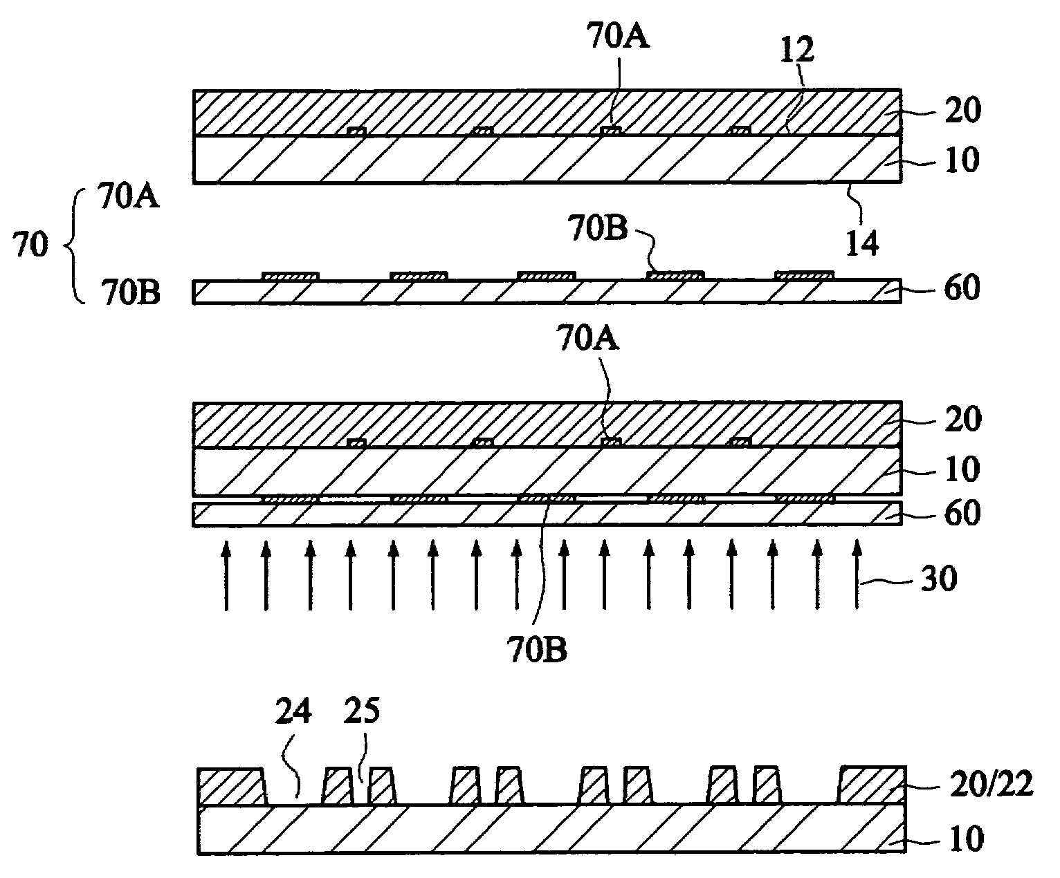
[0019]FIGS. 3A to 3G are schematic illustrations showing a method of manufacturing a LIGA mold by backside exposure according to the invention. As shown in FIG. 3A, a first substrate 10, which is transparent to a predetermined light source and has a front side 12 and a backside 14, is provided. The predetermined light source may be, for example, an ultra-violet light source, a laser source, an excimer laser source, an X-ray or synchronous radiation X-ray source. The first substrate may be made of, for example, quartz, soda glass, a polymeric material, a cyclo olefin copolymer (COC) or silicon. Then, a photoresist layer 20 is formed on a side (e.g., the front side 12) of the first substrate 10 by way of, for example, spin coating. In this embodiment, the photoresist layer 20 is a negative photoresist layer made of, for example, an SU-8 resist, and the predetermined light source is the ultra-violet light source. Then, a mask layer 70 is disposed on a side of the first substrate 10. Th...
third embodiment
[0022]FIG. 5 is a schematic illustration partially showing a method of manufacturing a LIGA mold by backside exposure according to the invention. As shown in FIG. 5, the mask layer 70 is formed on the backside 14 of the first substrate 10. The mask layer 70 may be formed before or after the photoresist layer 20 is formed.
fourth embodiment
[0023]FIGS. 6A and 6B are schematic illustration partially showing a method of manufacturing a LIGA mold by backside exposure according to the invention. As shown in FIGS. 6A and 6B, the mask layer 70 is formed on the front side 12 of the first substrate 10. Then, the photoresist layer 20 is formed on the first substrate 10.
PUM
| Property | Measurement | Unit |
|---|---|---|
| transparent | aaaaa | aaaaa |
| aspect ratio | aaaaa | aaaaa |
| optical property | aaaaa | aaaaa |
Abstract
Description
Claims
Application Information
 - R&D
- Intellectual Property
- Life Sciences
- Materials
- Tech Scout
- Unparalleled Data Quality
- Higher Quality Content
- 60% Fewer Hallucinations
Browse by: Latest US Patents, China's latest patents, Technical Efficacy Thesaurus, Application Domain, Technology Topic, Popular Technical Reports.
© 2025 PatSnap. All rights reserved.Legal|Privacy policy|Modern Slavery Act Transparency Statement|Sitemap|About US| Contact US: help@patsnap.com


