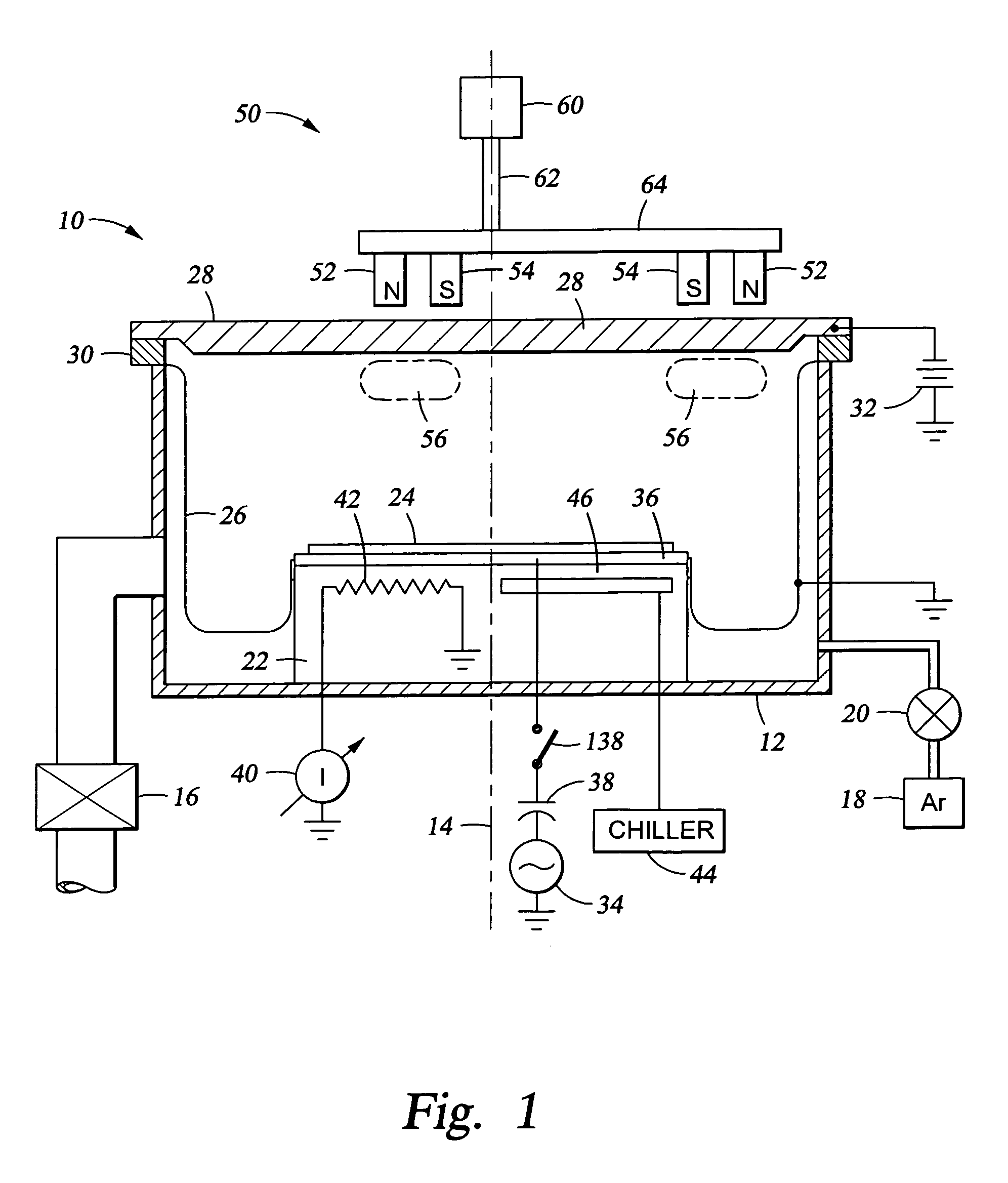
Aluminum sputtering while biasing wafer
a sputtering and aluminum technology, applied in the field of two-step aluminum sputtering process, can solve the problems of large unbalanced magnetron, large unbalanced magnetron, and general isotropic flux pattern of neutral sputter atoms unsuitable for filling high aspect-ratio holes, and achieve high substrate bias and promote adhesion to dielectric sidewalls
- Summary
- Abstract
- Description
- Claims
- Application Information
AI Technical Summary
Benefits of technology
Problems solved by technology
Method used
Image

Examples
Embodiment Construction
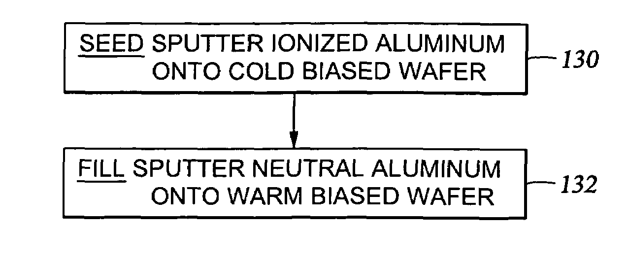
[0029]In one aspect of the invention and, illustrated in the cross-sectional view of an aluminum metallization structure in FIG. 5, an aluminum sputter fill process is divided into the sputter deposition of a thin aluminum seed layer 120 and a subsequent sputter deposition of a thicker aluminum fill layer 122. The deposition of these two different layers 120, 122 having significantly different characteristics is achieved by a significant change of the sputtering conditions between the two steps.
[0030]A broad aspect of the invention includes a cold, biased sputter deposition process for depositing aluminum, for example, to form the thin, nearly conformal seed layer 120 deep within a narrow hole while the wafer 24 is biased negatively to draw ionized aluminum sputter atoms deep within the hole and also while the wafer 24 is maintained at a relatively low temperature so that the aluminum sputter atoms stick to the barrier layer 108 on the hole sidewalls.
[0031]The cold, biased aluminum ...
PUM
| Property | Measurement | Unit |
|---|---|---|
| diameter | aaaaa | aaaaa |
| temperature | aaaaa | aaaaa |
| temperature | aaaaa | aaaaa |
Abstract
Description
Claims
Application Information
 - R&D
- Intellectual Property
- Life Sciences
- Materials
- Tech Scout
- Unparalleled Data Quality
- Higher Quality Content
- 60% Fewer Hallucinations
Browse by: Latest US Patents, China's latest patents, Technical Efficacy Thesaurus, Application Domain, Technology Topic, Popular Technical Reports.
© 2025 PatSnap. All rights reserved.Legal|Privacy policy|Modern Slavery Act Transparency Statement|Sitemap|About US| Contact US: help@patsnap.com