
Method and system for forming a feature in a high-k layer

a technology of high-k layer and feature, applied in the field of semiconductor processing, can solve the problems of process development and integration issues, oxide interface layer may need to be thin, and the overall dielectric constant of the gate stack, so as to reduce the formation of oxide interface layer, improve operational and/or reliability characteristics, and reduce the negative electrostatic charge

Inactive Publication Date: 2008-04-22
TOKYO ELECTRON LTD
View PDF26 Cites 2 Cited by
  • Summary
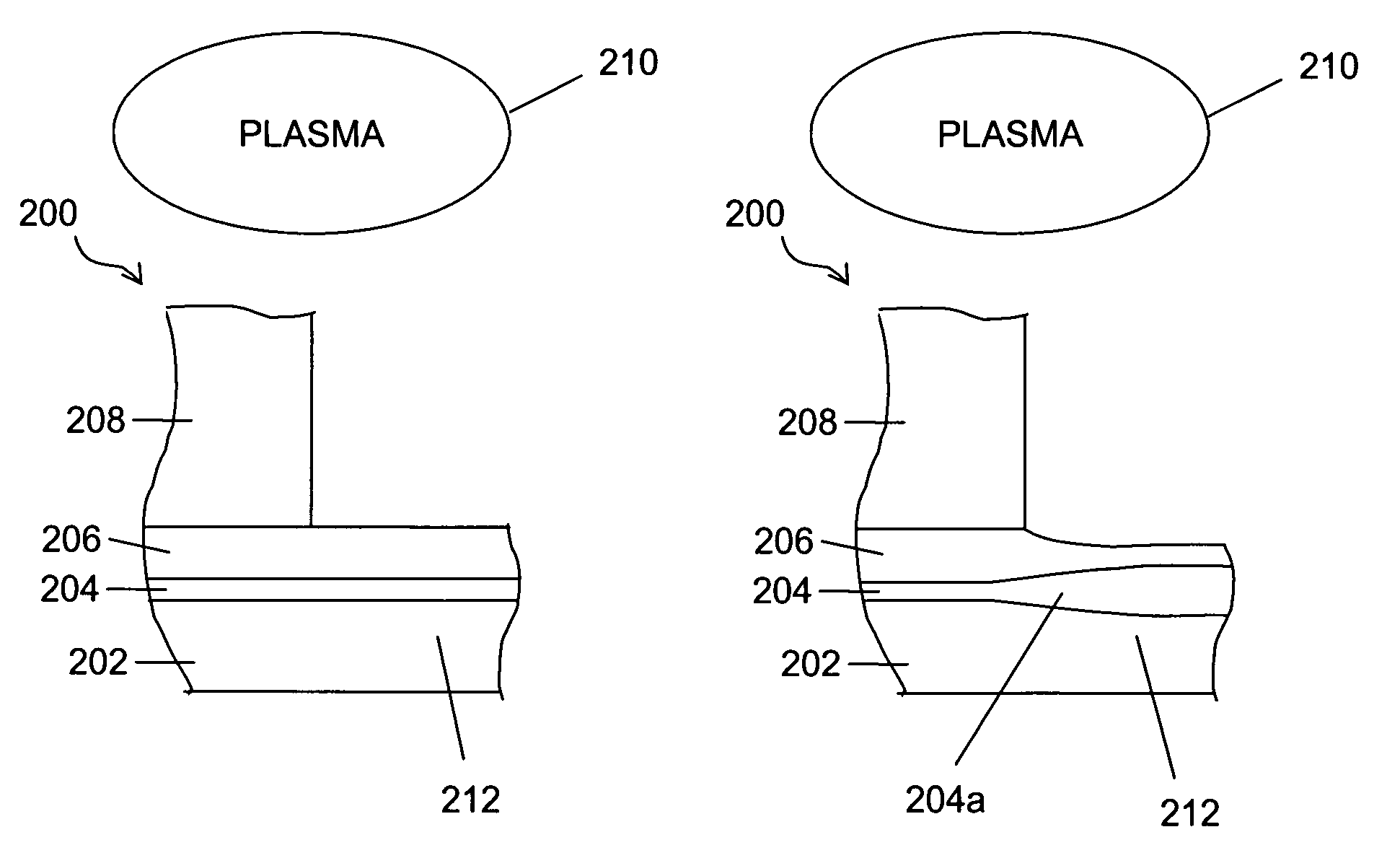
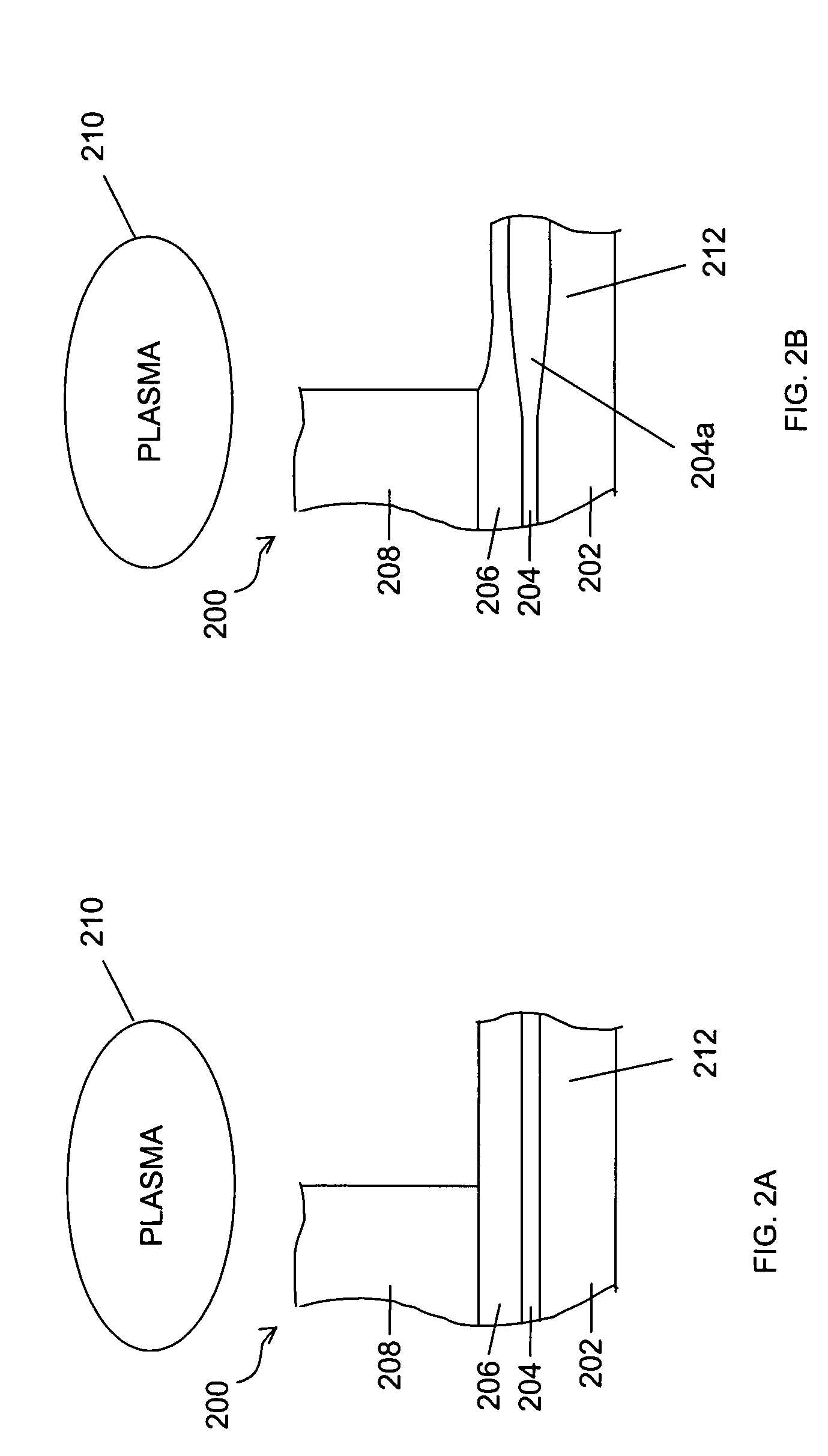
  • Abstract
  • Description
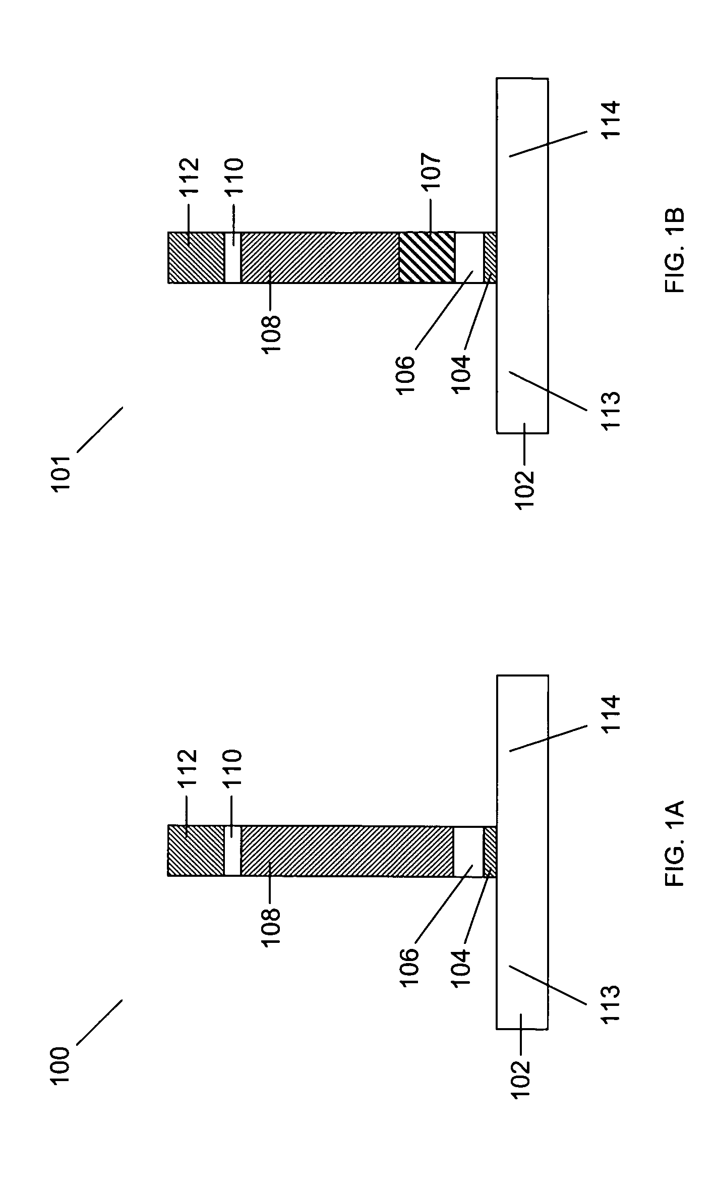
  • Claims
  • Application Information

AI Technical Summary

Benefits of technology

[0005]Accordingly, one object of the present invention is to provide an improved system and method for forming features in a high-k layer.
[0006]Another object of the present invention is to provide an electronic device having improved operational and / or reliability characteristics.
[0007]These and / or other object of the invention can be achieved by a method and system for plasma processing a high-k layer. The method includes reducing formation of an oxide interface layer during plasma processing of a substrate having a high-k layer formed thereon. According to embodiments of the invention, reducing the negative electrostatic charge on the surface of the high-k layer during anisotropic plasma processing, is found to reduce the formation of an oxide interface layer which in turn can improve the etch profile of the high-k layer and reduce oxidation of the substrate.
[0008]In one aspect of the invention, a method for plasma processing a high-k layer includes providing a substrate having a high-k layer formed thereon, on a substrate holder in a process chamber, and creating a plasma in the process chamber to thereby expose the high-k layer to the plasma. RF power is applied to the substrate holder, the RF power having a characteristic to reduce a rate of formation of an oxide interface layer located between the substrate and the high-k layer.
[0009]In another aspect of the invention, a method for plasma processing a gate stack includes providing, on a substrate holder in a process chamber, a gate stack containing a substrate having an interface layer formed on the substrate, a high-k layer formed on the interface layer, and a patterned gate electrode layer formed on the high-k layer, and creating a plasma in the process chamber to thereby expose the high-k layer to the plasma in an anisotropic etch process. RF power is applied to the substrate holder, the RF power having a characteristic to reduce a rate of formation of an oxide interface layer located between the substrate and the high-k layer next to the gate stack.

Problems solved by technology

Thus, process development and integration issues are key challenges for new gate stack materials and silicide processing.
However, the presence of an oxide interface layer lowers the overall dielectric constant of the gate stack and, therefore, the oxide interface layer may need to be thin.
These aggressive etch processes, however, can lead to removal of the substrate material itself, which can result in poor device characteristics.
While these efforts have led to control of overetching high-k layers, the present inventors have recognized that devices having features formed in high-k materials can still suffer from reliability and / or operational problems.

Method used


Image

  • Method and system for forming a feature in a high-k layer
  • Method and system for forming a feature in a high-k layer
  • Method and system for forming a feature in a high-k layer

Examples


example

Plasma Etching of a HfO2 High-K Layer using HBr Plasma

[0058]A gate stack containing a 40 Å thick HfO2 high-k layer overlying a 5 Å thick SiOxNy interface layer on a Si substrate was exposed to a plasma containing a HBr etch gas. The process conditions included a HBr gas flow rate of 400 sccm and a process chamber pressure of 20 mTorr. The plasma processing system was a capacitively coupled plasma system as schematically shown in FIG. 5. The present inventors found that providing 40 W of power on the substrate holder can remove the HfO2 at 370° C.; however, swelling of the interfacial layer still existed. Thus, the present inventors selected an RF power that further reduces the oxide swelling in accordance with the present invention. In this example, the top electrode power was reduced from 1,000 W to 200 W and the RF power applied to the substrate holder was increased from 40 W to 50 W.

[0059]FIG. 9 shows a TEM image of a gate stack following plasma processing of the gate stack accor...


PUM


Abstract

A method for plasma processing a high-k layer includes providing a substrate having a high-k layer formed thereon, on a substrate holder in a process chamber, and creating a plasma in the process chamber to thereby expose the high-k layer to the plasma. RF power is applied to the substrate holder, the RF power having a characteristic to reduce a rate of formation of an oxide interface layer located between the substrate and the high-k layer. A device includes a feature etched in a high-k layer. The etch profile of the device can include a reduced bird's beak, and a surface of the substrate in an etched region can be substantially coplanar with a substrate under a non-etched area.

Description

FIELD OF THE INVENTION[0001]The present invention is related to semiconductor processing, and more particularly, to a method and system for forming a feature in a high-k layer formed on a substrate.BACKGROUND OF THE INVENTION[0002]In the semiconductor industry, the minimum feature sizes of microelectronic devices are approaching the deep sub-micron regime to meet the demand for faster, lower power microprocessors and digital circuits. This trend is leading, for example, to imminent replacement of SiO2 and Si-oxynitride (SiOxNy) dielectric materials with high-permittivity dielectric materials (also referred to herein as “high-k” materials), and the use of alternative gate electrode materials to replace the traditional doped polycrystalline silicon (poly-Si) in sub-0.1 μm complementary metal-oxide semiconductor (CMOS) technology. Thus, process development and integration issues are key challenges for new gate stack materials and silicide processing.[0003]Dielectric materials featuring...

Claims


Application Information

Patent Timeline
Patent Type & Authority Patents(United States)
IPC IPC(8): H01L21/302H01L21/461
CPCH01J37/32706H01L21/31116H01L21/31122H01L21/31645H01L29/517H01L21/0234
Inventor KO, AKITERUXIA, ANNIECHEN, LEE
Owner TOKYO ELECTRON LTD
Learn More