
Semiconductor memory device having self-aligned charge trapping layer

a memory device and self-aligning technology, applied in the direction of semiconductor devices, electrical appliances, transistors, etc., can solve the problems of high initial threshold voltage, high programming current, and high programming current, so as to avoid the problem of conventional local sonos nonvolatile memory devices

Inactive Publication Date: 2008-03-18
SAMSUNG ELECTRONICS CO LTD
View PDF14 Cites 7 Cited by
  • Summary
  • Abstract
  • Description
  • Claims
  • Application Information

AI Technical Summary

Benefits of technology

[0018]The present invention also provides a method of manufacturing a semiconductor memory device comprising a self-aligned charge trapping layer in which variations in length of an ONO layer caused by misalignment are prevented.

Problems solved by technology

For this reason, the SONOS nonvolatile memory device has a high initial threshold voltage, a correspondingly high electric power dissipation, and high programming current.
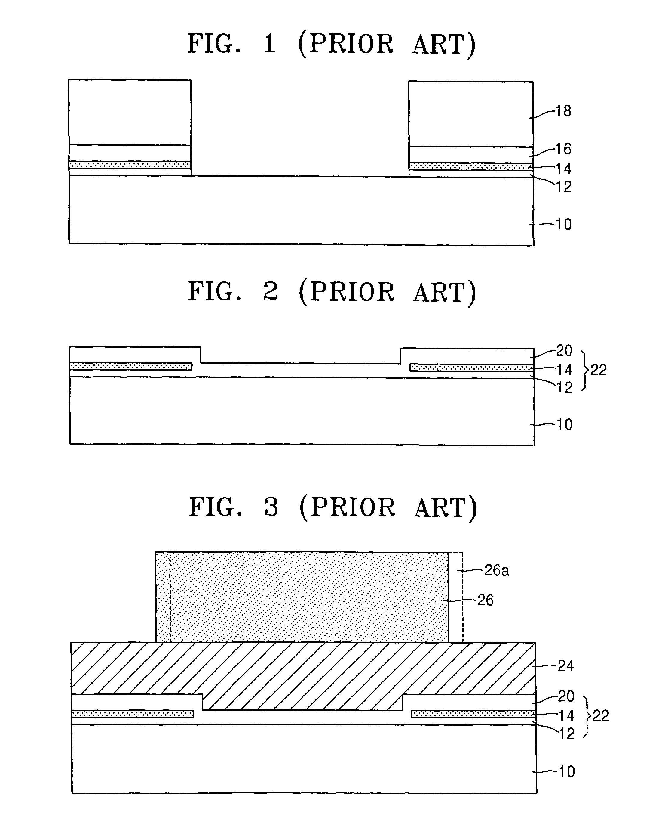
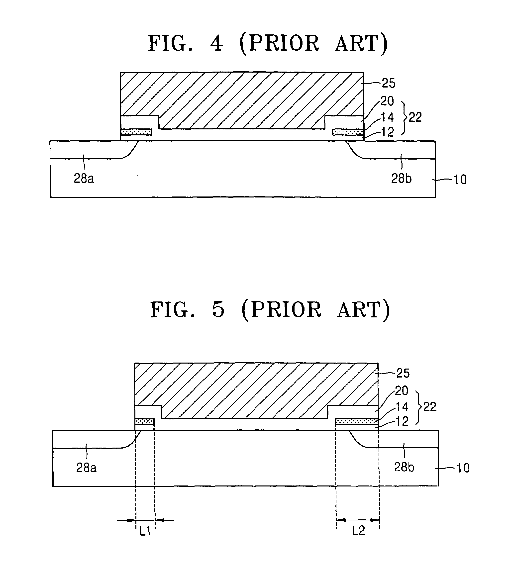
However, the foregoing conventional local SONOS nonvolatile memory device experiences problems resulting from the inconsistent formation of ONO layer 22 using the foregoing photolithography process.

Method used


Image

  • Semiconductor memory device having self-aligned charge trapping layer
  • Semiconductor memory device having self-aligned charge trapping layer
  • Semiconductor memory device having self-aligned charge trapping layer

Examples


Embodiment Construction

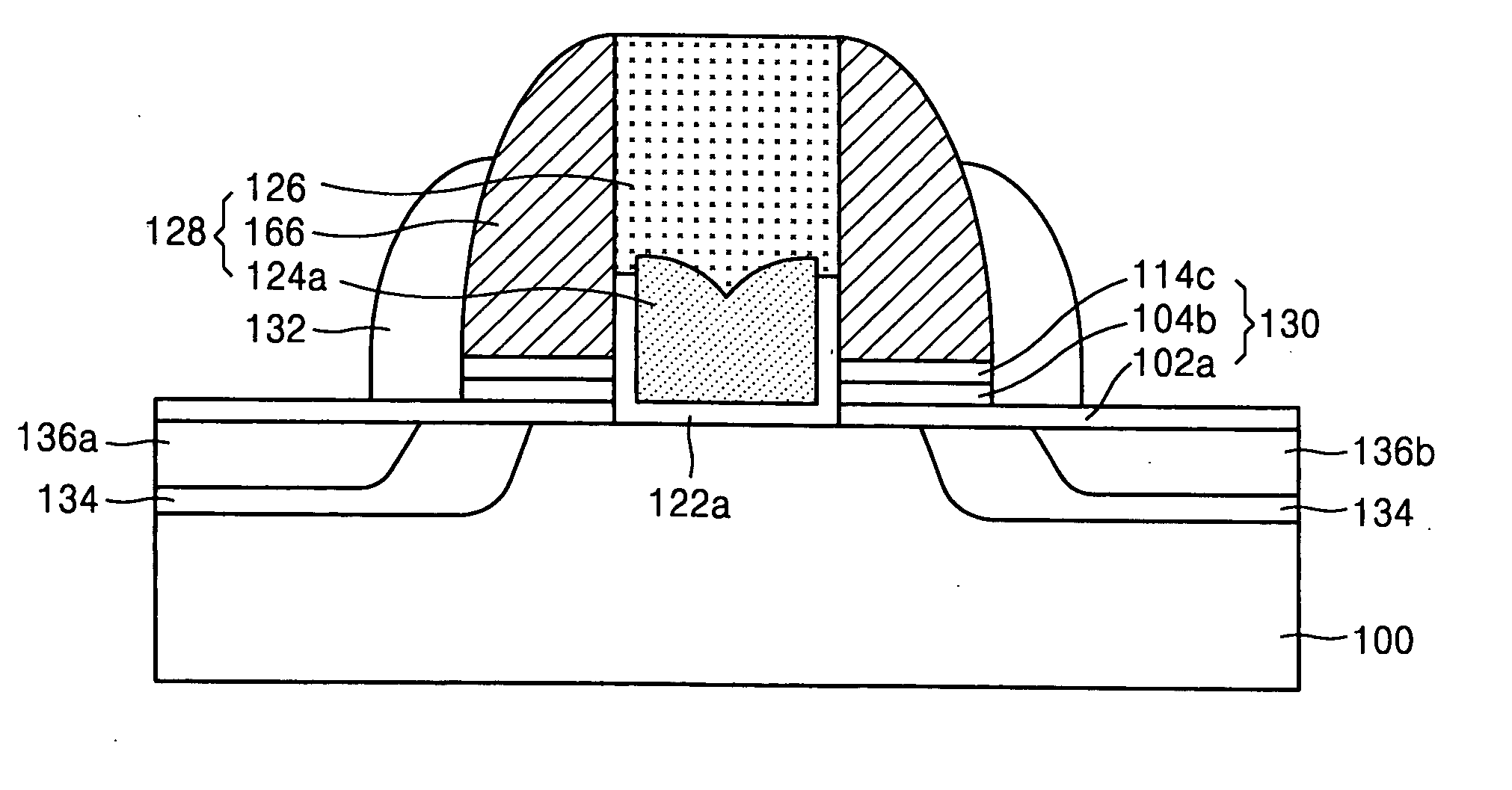
[0035]The length of a charge trapping layer in a semiconductor memory device according to the present invention is determined in one aspect by self-alignment using a conductive spacer. By doing so, the length of the charge trapping layer is defined without the use of a plurality of photolithography processes. As a result, length variations in the charge trapping layer caused by photolithography misalignments are prevented. The present invention will be described in conjunction with a 2-bit cell structure, in which a single gate includes two charge trapping layers. However, this is just a selected teaching example. The present invention is not limited to a 2-bit cell structure.

[0036]FIG. 6 is a sectional view showing a semiconductor memory device including a self-aligned charge trapping layer according to one presently preferred embodiment of the invention.

[0037]Referring to FIG. 6, the memory device includes semiconductor substrate 100 having source and drain regions 136a and 136b. ...


PUM


Abstract

A semiconductor memory device having a self-aligned charge trapping layer and a method of manufacturing the same in which a consistent length of an ONO layer is ensured. Here, an insulating stacked structure is self-aligned to a bottom surface of conductive spacers.

Description

BACKGROUND OF THE INVENTION[0001]1. Field of the Invention[0002]The present invention relates to a semiconductor memory device and a method of manufacturing the same. More particularly, the present invention relates to a semiconductor memory device having a charge trapping layer formed via self-alignment and a method of manufacturing the same.[0003]A claim of priority is made to Korean Patent Application No. 2003-92502 filed on Dec. 17, 2003, the disclosure of which is incorporated herein by reference in its entirety.[0004]2. Description of the Related Art[0005]A nonvolatile memory device retains stored data even in the absence of a power supply. A Silicon-Oxide-Nitride-Oxide-Silicon (SONOS) nonvolatile memory device with an Oxide-Nitride-Oxide (ONO) structure capable of trapping charges and having a single MOSFET gate electrode is disclosed, for example, in U.S. Pat. No. 5,768,192. The SONOS nonvolatile memory device is readily manufactured and integrated within a peripheral region...

Claims


Application Information

Patent Timeline
Patent Type & Authority Patents(United States)
IPC IPC(8): H01L29/792H01L21/8247H01L21/28H01L21/336H01L21/8246H01L27/115H01L29/788
CPCH01L21/28282H01L27/115H01L27/11568H01L29/66833H01L29/7923H01L29/40117H10B69/00H10B43/30
Inventor JEON, HEE-SEOGYOON, SEUNG-BEOMKIM, YONG-TAE
Owner SAMSUNG ELECTRONICS CO LTD
Learn More