
Split gate flash memory device having self-aligned control gate and method of manufacturing the same

a self-aligning, flash memory device technology, applied in the field of flash memory devices, can solve the problems of more difficult scaling down of split gate flash memory devices than stacked flash memory devices, and achieve the effect of reducing cell size and enhancing electric field

Inactive Publication Date: 2008-03-11
SAMSUNG ELECTRONICS CO LTD
View PDF14 Cites 8 Cited by
  • Summary
  • Abstract
  • Description
  • Claims
  • Application Information

AI Technical Summary

Benefits of technology

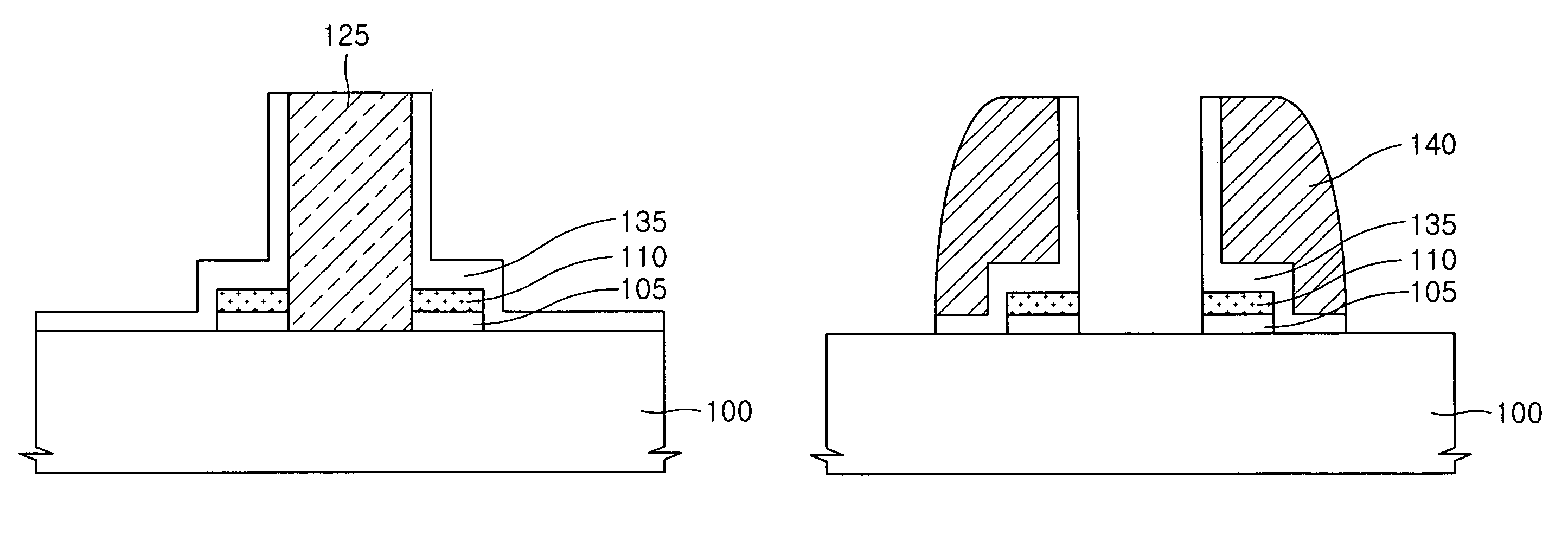
The present invention provides a flash memory device that can maintain an enhanced electric field between the control gate and the storage node while reducing the cell size. The device includes a semiconductor substrate with a source region and a drain region, and a spacer-shaped control gate and a storage node formed between the control gate and the semiconductor substrate. The control gate has a first conductive spacer that overlaps with the semiconductor substrate and a second conductive spacer that overlaps with the storage node. The device also includes an insulating layer between the storage node and the control gate and between the storage node and the semiconductor substrate. The method of manufacturing the flash memory device involves forming a storage node layer on a semiconductor substrate, sequentially stacking a semiconductor tunnel oxide layer, a storage node layer, a first gate insulating layer, and a damascene molding layer, and removing dummy spacers. The device has a smaller cell size and uniform overlap length between the control gate and the storage node.

Problems solved by technology

Accordingly, it is more difficult to scale down the split gate flash memory device as compared to the stacked flash memory device.

Method used


Image

  • Split gate flash memory device having self-aligned control gate and method of manufacturing the same
  • Split gate flash memory device having self-aligned control gate and method of manufacturing the same
  • Split gate flash memory device having self-aligned control gate and method of manufacturing the same

Examples


Embodiment Construction

[0035]The present invention will now be described more fully with reference to the accompanying drawings, in which preferred embodiments of the invention are shown. The invention may, however, be embodied in many different forms and should not be construed as being limited to the embodiments set forth herein. Rather, these embodiments are provided so that this disclosure will be thorough and complete. In the drawings, the thicknesses of layers and regions and the sizes of components may be exaggerated for clarity, and the same elements are given the same reference numerals throughout the drawings.

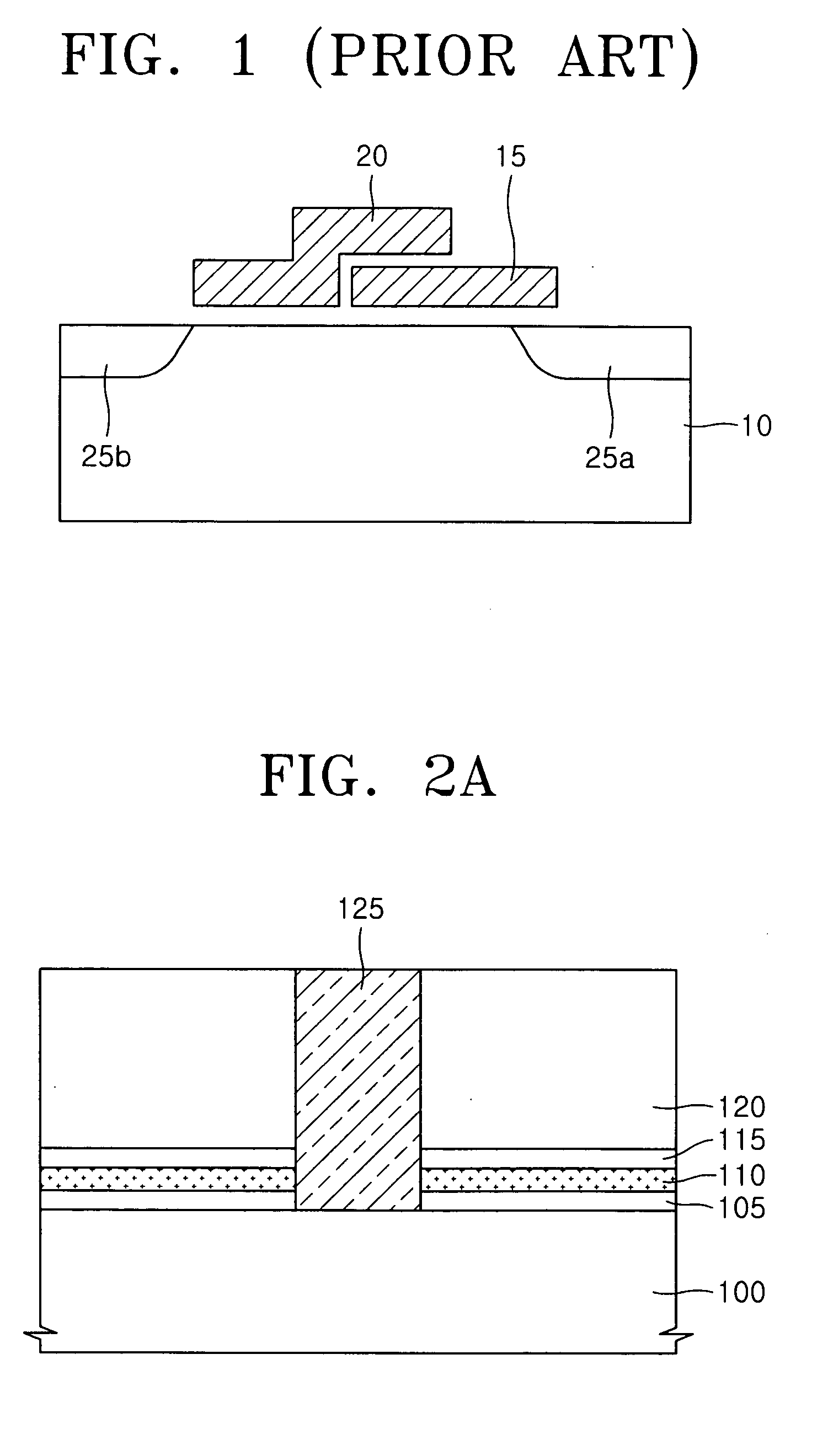
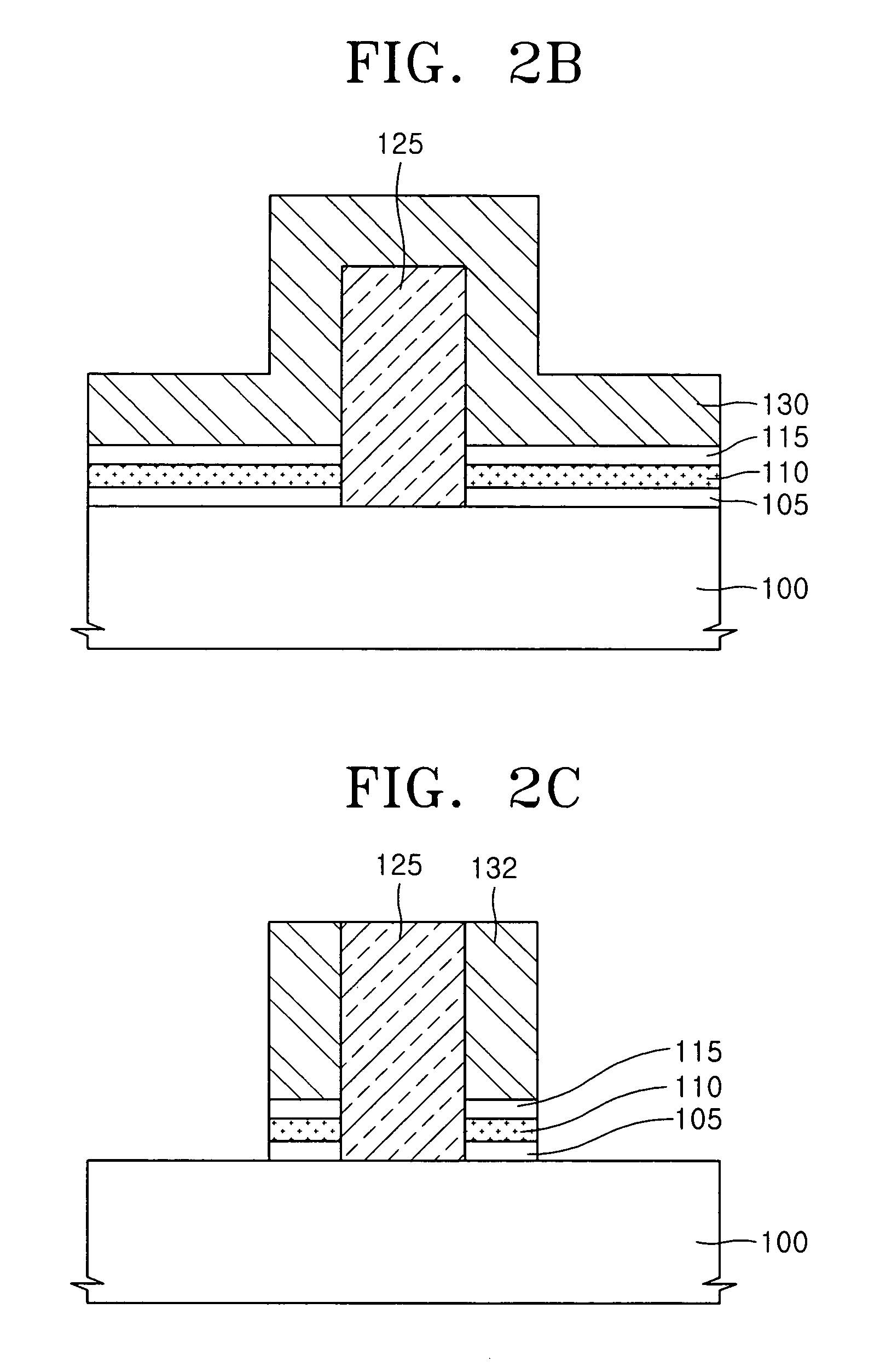
[0036]FIGS. 2A through 2E are cross-sectional views illustrating a method of manufacturing a flash memory device according to an embodiment of the present invention.

[0037]Referring to FIG. 2A, a tunnel oxide layer 105, a storage node 110, and a first gate insulating layer 115 are sequentially deposited on a semiconductor substrate 100. The semiconductor substrate 100 comprises, for example,...


PUM


Abstract

In a flash memory device, which can maintain an enhanced electric field between a control gate and a storage node (floating gate) and has a reduced cell size, and a method of manufacturing the flash memory device, the flash memory device includes a semiconductor substrate having a pair of drain regions and a source region formed between the pair of drain regions, a pair of spacer-shaped control gates each formed on the semiconductor substrate between the source region and each of the drain regions, and a storage node formed in a region between the control gate and the semiconductor substrate. A bottom surface of each of the control gates includes a first region that overlaps with the semiconductor substrate and a second region that overlaps with the storage node. The pair of spacer-shaped control gates are substantially symmetrical with each other about the source region.

Description

BACKGROUND OF THE INVENTION[0001]This application claims the priority of Korean Patent Application No. 10-2005-0015041, filed on Feb. 23, 2005, in the Korean Intellectual Property Office, the disclosure of which is incorporated herein in its entirety by reference.[0002]1. Field of the Invention[0003]The present invention relates to a flash memory device and a method of manufacturing the same, and more particularly, to a split gate flash memory device having a self-aligned control gate and a method of manufacturing the same.[0004]2. Description of the Related Art[0005]Non-volatile semiconductor devices electrically store and erase data and can retain data even when power is turned off. Accordingly, non-volatile semiconductor devices enjoy widespread use in various fields, including portable electronics.[0006]As one type of non-volatile memory device, a split gate flash memory device includes a floating gate (or a storage node) and a control gate that are separated from each other. Th...

Claims


Application Information

Patent Timeline
Patent Type & Authority Patents(United States)
IPC IPC(8): H01L21/336H10B69/00
CPCH01L29/42324H01L29/66825H01L29/66833H01L29/7881H01L29/792H01L21/76897
Inventor CHOI, BYUNG-YONGOH, CHANG-WOOPARK, DONG-GUNKIM, DONG-WONLEE, YONG-KYU
Owner SAMSUNG ELECTRONICS CO LTD
Learn More