Power amplifier and transmitter
a power amplifier and transmitter technology, applied in the field of power amplifiers, can solve the problems of low power efficiency, low power efficiency, and apparent decrease in load resistance, and achieve the effect of simple structure and high power efficiency
- Summary
- Abstract
- Description
- Claims
- Application Information
AI Technical Summary
Benefits of technology
Problems solved by technology
Method used
Image
Examples
first embodiment
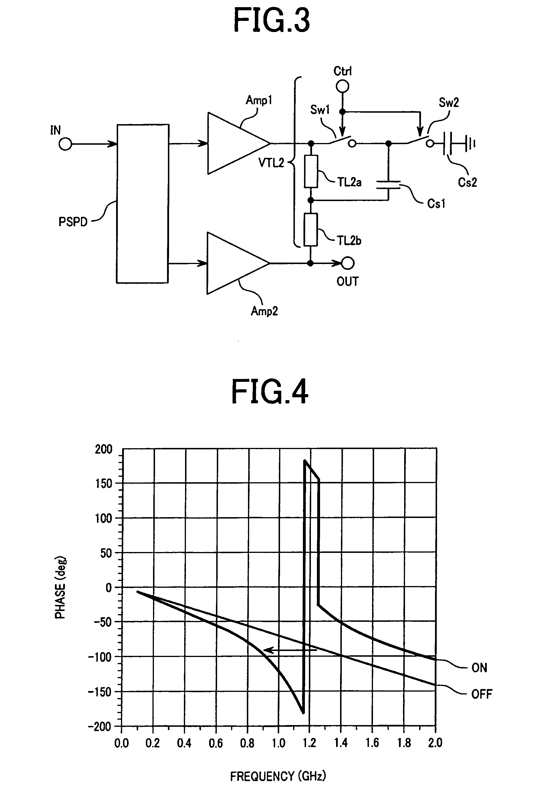
[0055]Next, a first embodiment according to the present invention will be described in detail with reference to FIGS. 3 to 6.
[0056]FIG. 3 is a circuit diagram of a Doherty type amplifier of the first embodiment of the present invention.
[0057]FIG. 4 is a graphical representation showing a relationship between frequency and phase delay of the output power combiner of the Doherty type amplifier of the first embodiment of the present invention.
[0058]FIG. 5 is an equivalent circuit diagram of a transmission line.
[0059]FIG. 6 is an equivalent circuit diagram of a variable electric length circuit of the first embodiment of the present invention.
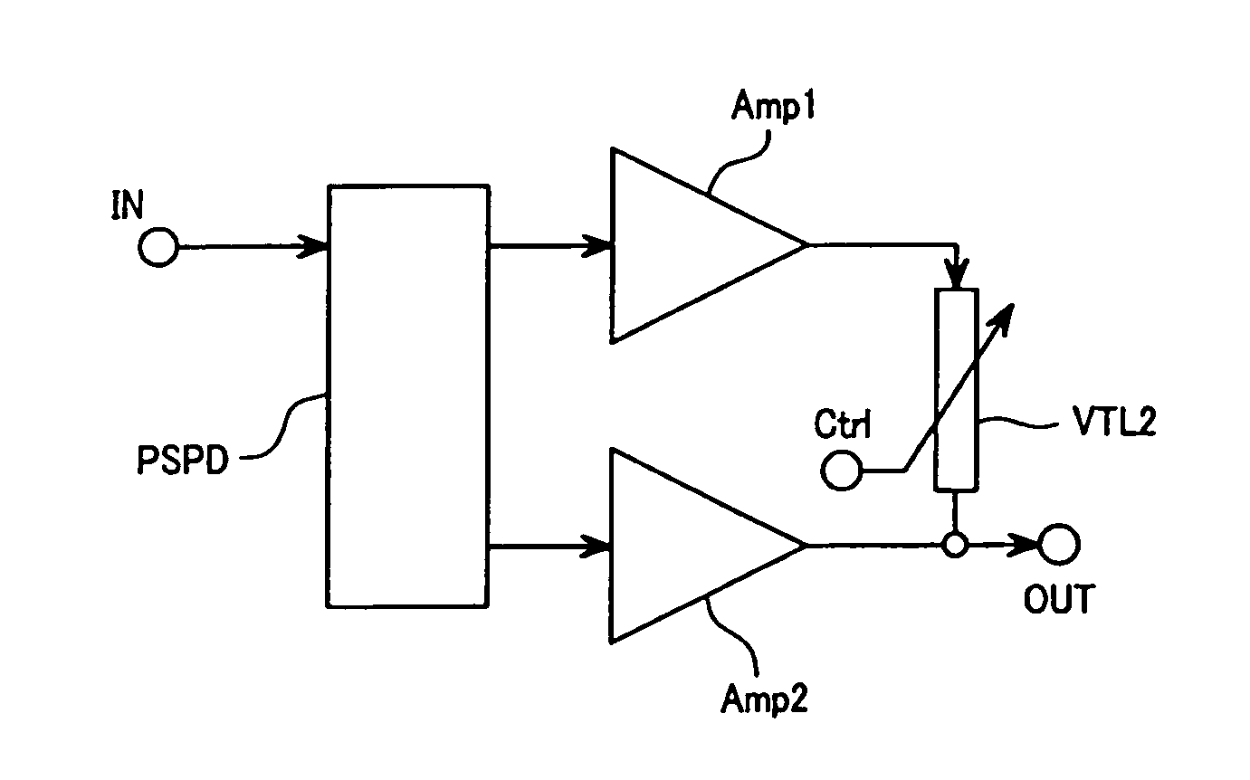
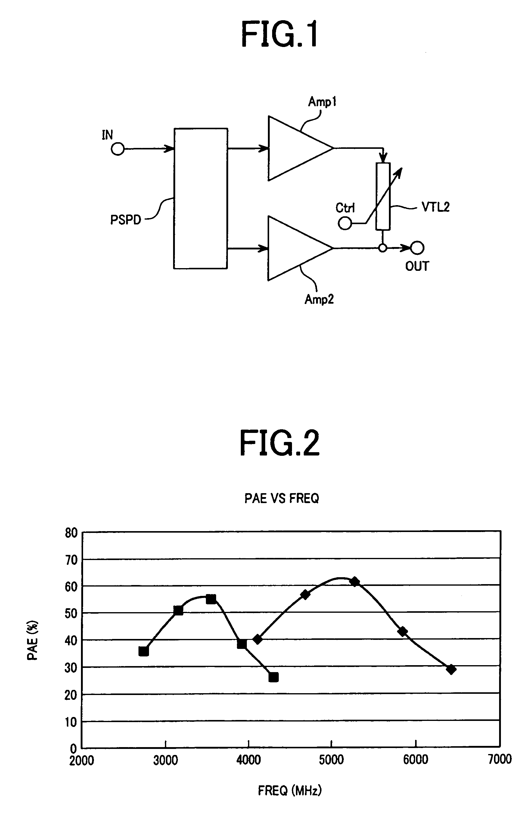
[0060]The first embodiment shows a more concrete circuit for realizing the variable electric length power combiner VTL2 shown in FIG. 1. The carrier amplifier Amp1, the peak amplifier Amp2, and the 90-degree phase-shift power divider PSPD are the same as those in the outline described with reference to FIG. 1.
[0061]Here, it is assumed that the band ...
second embodiment
[0068]Next, a second embodiment according to the present invention will be described in detail with reference FIG. 7.
[0069]FIG. 7 is a circuit diagram of a Doherty type amplifier of the second embodiment of the present invention.
[0070]In the second embodiment, the switches of the first embodiment are replaced with FET elements, respectively.
[0071]The carrier amplifier Amp1 of the Doherty type amplifier of the second embodiment of the present invention, as shown in FIG. 7, is constituted by an FET element Mc and a dc-block capacitor Cc1. A drain terminal, a source terminal, and a gate terminal of the FET element Mc are connected to a power source voltage terminal Vdc, a ground, and a bias voltage terminal Vgc, respectively. The dc-block capacitor Cc1 is connected between the 90-degree phase-shift power divider PSPD and the gate terminal of the FET element Mc.
[0072]The peak amplifier Amp2 is constituted by an FET element Mp and a dc-block capacitor Cp1. A drain terminal, a source term...
third embodiment
[0079]Next, a third embodiment according to the present invention will be described in detail with reference to FIG. 8.
[0080]FIG. 8 is a circuit diagram of a Doherty type amplifier of the third embodiment of the present invention.
[0081]In the third embodiment, the carrier amplifier Amp1 and the peak amplifier Amp2 of the second embodiment are constituted by bipolar elements instead of FET elements.
[0082]The carrier amplifier Amp1 of the third embodiment, as shown in FIG. 8, is constituted by a bipolar element Bc and the dc-block capacitor Cc1. A collector terminal, an emitter terminal, and a base terminal of the bipolar element Bc are connected to a power source voltage terminal Vdc, a ground, and a bias voltage terminal Vgc, respectively. The dc-block capacitor Cc1 is connected between the 90-degree phase-shift power divider PSPD and the base terminal of the bipolar element Bc.
[0083]The peak amplifier Amp2 is constituted by a bipolar element Bp and a dc-block capacitor Cp1. A colle...
PUM
 Abstract
Description
Claims
Application Information
 - R&D
- Intellectual Property
- Life Sciences
- Materials
- Tech Scout
- Unparalleled Data Quality
- Higher Quality Content
- 60% Fewer Hallucinations
Browse by: Latest US Patents, China's latest patents, Technical Efficacy Thesaurus, Application Domain, Technology Topic, Popular Technical Reports.
© 2025 PatSnap. All rights reserved.Legal|Privacy policy|Modern Slavery Act Transparency Statement|Sitemap|About US| Contact US: help@patsnap.com


