Nitride-based compound semiconductor electron device including a buffer layer structure
a compound semiconductor and electron device technology, applied in the field of nitride-based compound semiconductor electron device, can solve the problems of degrading the pinch-off characteristic, difficult to form a semiconductor layer structure in a gan-based fet, and difficult to manufacture a single-crystal substrate having a large diameter in the case of gan-based crystals in different ways, etc., to achieve excellent pinch-off characteristic, suppress leakage current, and different material quality
- Summary
- Abstract
- Description
- Claims
- Application Information
AI Technical Summary
Benefits of technology
Problems solved by technology
Method used
Image
Examples
first embodiment
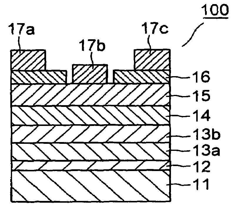
[0021]Referring to FIG. 1, a semiconductor electron device, generally designated by numeral 100, according to the present invention includes: a silicon substrate (semiconductor substrate) 11; a layer structure including a GaN intermediate layer 12, a pair of buffer layers including a first buffer layer 13a and a second buffer layer 13b, an GaN channel layer 14, an AlGaN donor layer 15, and a GaN contact layer, which are consecutively deposited on the silicon substrate 11; and an electrode group including an Al / Ti / Au source electrode 17a formed on the contact layer 16, a Pt / Au gate electrode 17b formed on the donor layer 15, and an Al / Ti / Au drain electrode 17c formed on the contact layer 16.
[0022]In the above structure, the first buffer layer 13a is made of GaN, and the second buffer layer 13b is made of AlGaN. The AlGaN second buffer layer 13b has a bandgap energy larger than the bandgap energy of the GaN first buffer layer 13a. The contact layer 16 formed on the donor layer 15 has ...
second embodiment
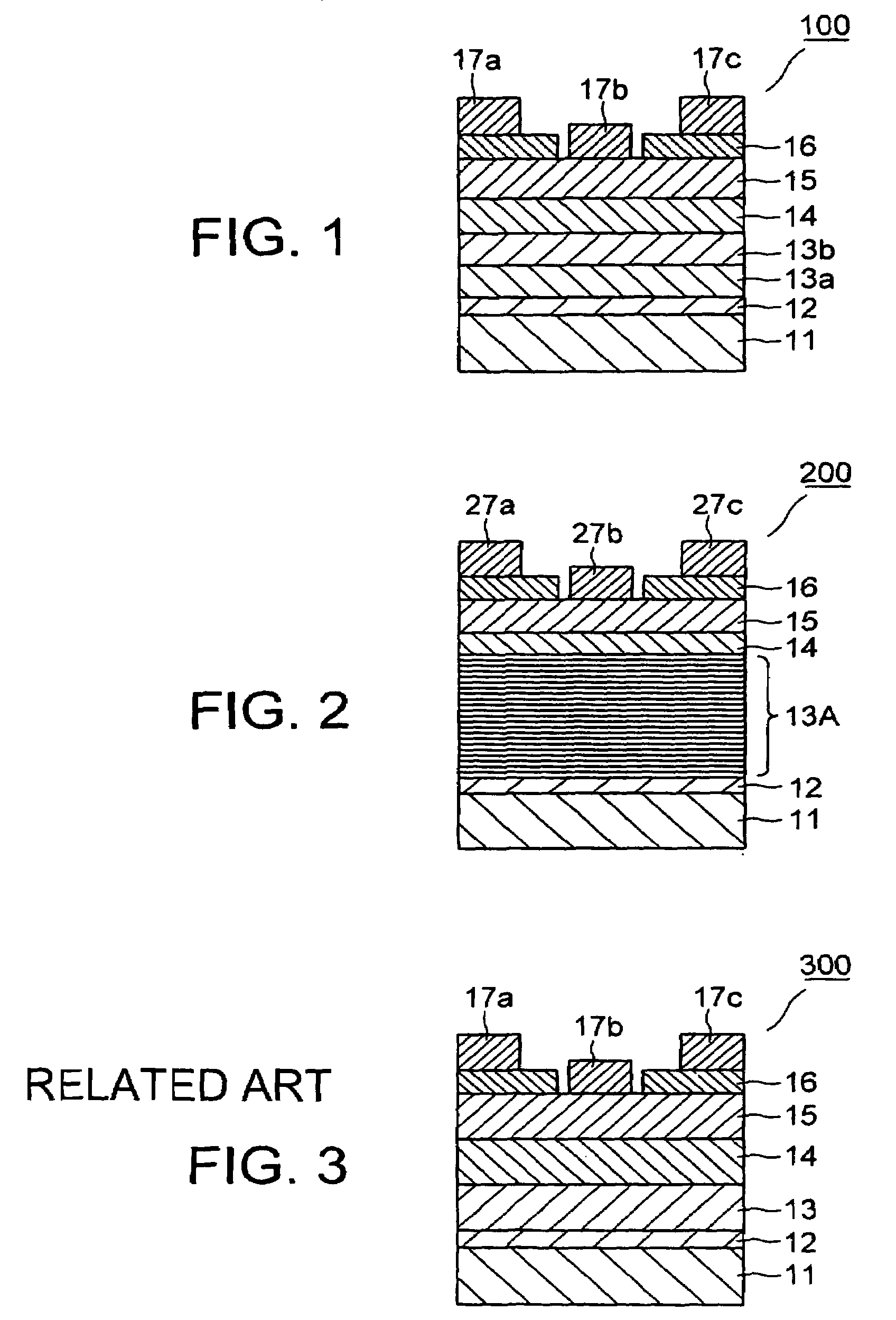
[0035]Referring to FIG. 2, a semiconductor electron device, generally designated by numeral 200, according to the present invention has a buffer layer structure 13A including 30 GaN first buffer layers and 30 AlGaN second buffer layers which are alternately deposited one on another on the intermediate layer 12.
[0036]More specifically, the semiconductor electron device 200 includes the silicon substrate 11, the intermediate layer 12, the channel layer 14, the donor layer 15, and the contact layer 16, which are deposited and configured similarly to those of the first embodiment with the exception of the buffer layer structure 13A.
[0037]In the buffer layer structure 13A, the GaN first buffer layers are designated herein by numerals 13an (13a1, 13a2 . . . 13a30), as viewed consecutively from the bottom, whereas AlGaN second buffer layers are designed herein by numerals 13bn (13b1, 13b2 . . . 13b30), as viewed consecutively from the bottom. It is to be noted that the AlGaN second buffer ...
PUM
 Abstract
Description
Claims
Application Information
 - R&D
- Intellectual Property
- Life Sciences
- Materials
- Tech Scout
- Unparalleled Data Quality
- Higher Quality Content
- 60% Fewer Hallucinations
Browse by: Latest US Patents, China's latest patents, Technical Efficacy Thesaurus, Application Domain, Technology Topic, Popular Technical Reports.
© 2025 PatSnap. All rights reserved.Legal|Privacy policy|Modern Slavery Act Transparency Statement|Sitemap|About US| Contact US: help@patsnap.com


