Semiconductor device
a semiconductor device and device technology, applied in the direction of semiconductor/solid-state device testing/measurement, semiconductor device details, semiconductor/solid-state device testing/measurement, etc., can solve the problem of inability to reduce the contour size of the sip down to a contour size, the defect analysis of the sdram cannot be performed, and the detailed evaluation, reliability test, and reliability analysis cannot be performed. to achieve the effect of reducing the contour size of the semiconductor devi
- Summary
- Abstract
- Description
- Claims
- Application Information
AI Technical Summary
Benefits of technology
Problems solved by technology
Method used
Image
Examples
embodiment 1
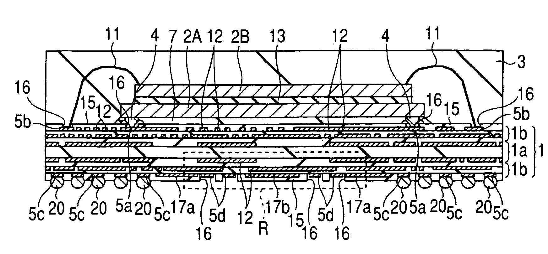
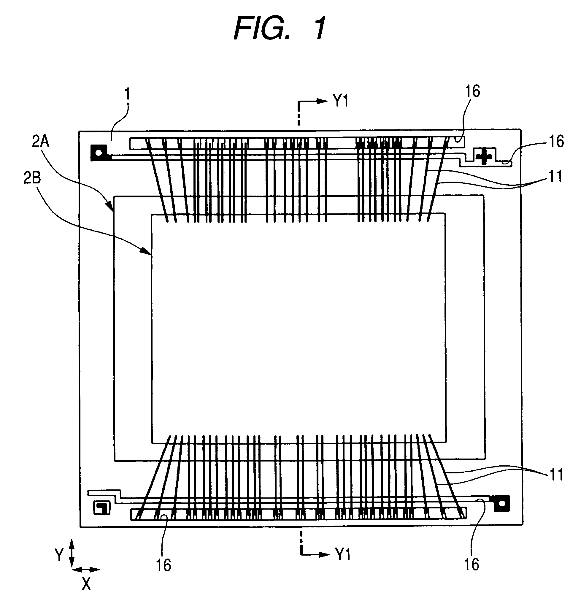
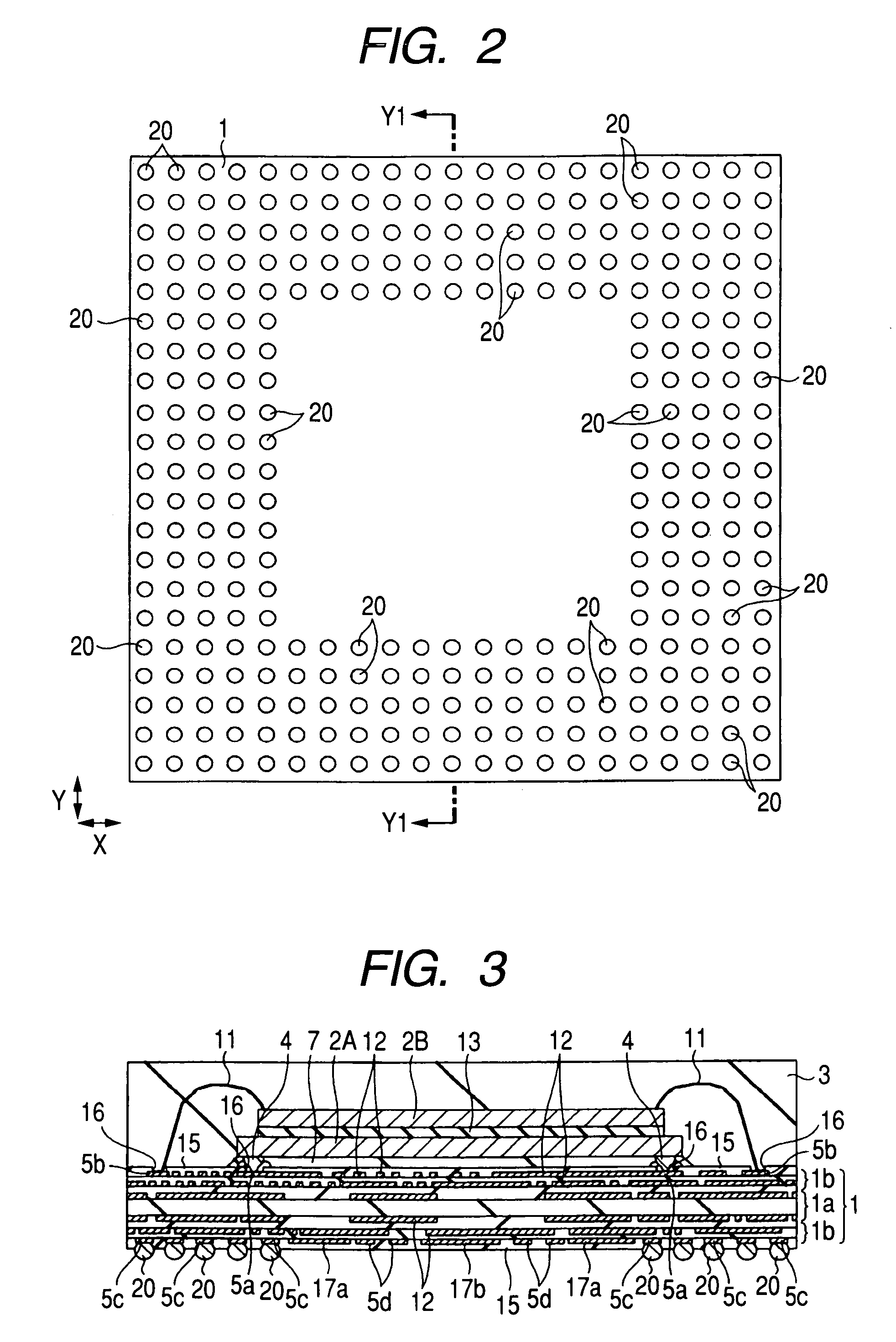
[0039]FIG. 1 is a plan view of the top plane (first main surface) of an interconnect substrate showing the internal structure of a semiconductor device of the present embodiment. FIG. 2 is a plan view of the bottom plane (second main surface) of the interconnect device of the semiconductor device shown in FIG. 1. FIG. 3 is a cross-sectional view taken on line Y1-Y1 of FIGS. 1 and 2. FIG. 4 is a plan view of a main surface of a second semiconductor chip of the semiconductor device shown in FIG. 1. FIG. 5 is a plan view of a main plane of a first semiconductor chip of the semiconductor device shown in FIG. 1. FIG. 6 is a table illustrating numbers given to the terminals of the first semiconductor chip shown in FIG. 5, as well as the names of the terminals. FIG. 7 is a plan view of the lowermost interconnect layer (second main surface) of the interconnect substrate of the semiconductor device shown in FIG. 1. FIG. 8 is a fragmentary plan view of the top-level interconnect layer (first ...
embodiment 2
[0063]FIG. 19 is a plan view of the bottom surface of a semiconductor device of the present Embodiment 2. FIG. 20 is a cross-sectional view taken on line Y2-Y2 of FIG. 19. FIG. 21 is an enlarged cross section of an area R of FIG. 20. FIG. 22 is a cross-sectional view of a modification of the device shown in FIG. 21.
[0064]In the present Embodiment 2, the surfaces of the electrodes 5d on the bottom surface of the interconnect substrate 1 of the semiconductor device are exposed from the solder resist 15. Openings 16 in which the electrodes 5d are exposed are formed simultaneously with when openings 16 in which the electrodes 5c are exposed are formed.
[0065]One method of exposing the electrodes 5d is to place the opening ends of the solder resist 15 remotely from the outer peripheries of the electrodes 5d such that the opening ends do not reach the outer peripheries (non solder mask defined (NSMD)) as shown in FIG. 21. Alternatively, the opening ends of the solder resist 15 may reach th...
PUM
 Abstract
Description
Claims
Application Information
 - R&D
- Intellectual Property
- Life Sciences
- Materials
- Tech Scout
- Unparalleled Data Quality
- Higher Quality Content
- 60% Fewer Hallucinations
Browse by: Latest US Patents, China's latest patents, Technical Efficacy Thesaurus, Application Domain, Technology Topic, Popular Technical Reports.
© 2025 PatSnap. All rights reserved.Legal|Privacy policy|Modern Slavery Act Transparency Statement|Sitemap|About US| Contact US: help@patsnap.com


