
Low voltage swing pad driver and receiver

a low-voltage swing pad and driver technology, applied in the field of low-voltage swing pad driver and receiver, can solve the problems of large injector of noise into the semiconductor device and system, and achieve the effects of reducing the distortion within the device, minimizing the distortion, and low noise operation

Inactive Publication Date: 2007-12-04
AVAGO TECH INT SALES PTE LTD
View PDF11 Cites 1 Cited by
  • Summary
  • Abstract
  • Description
  • Claims
  • Application Information

AI Technical Summary

Benefits of technology

Significantly reduces noise and distortion in semiconductor devices and systems, improving data accuracy and throughput by minimizing voltage swing at critical interfaces, thereby enhancing overall device and system performance.

Problems solved by technology

Undesirably voltage swing at such an interface may be a huge injector of noise into the semiconductor devices and system.

Method used


Image

  • Low voltage swing pad driver and receiver
  • Low voltage swing pad driver and receiver
  • Low voltage swing pad driver and receiver

Examples


Embodiment Construction

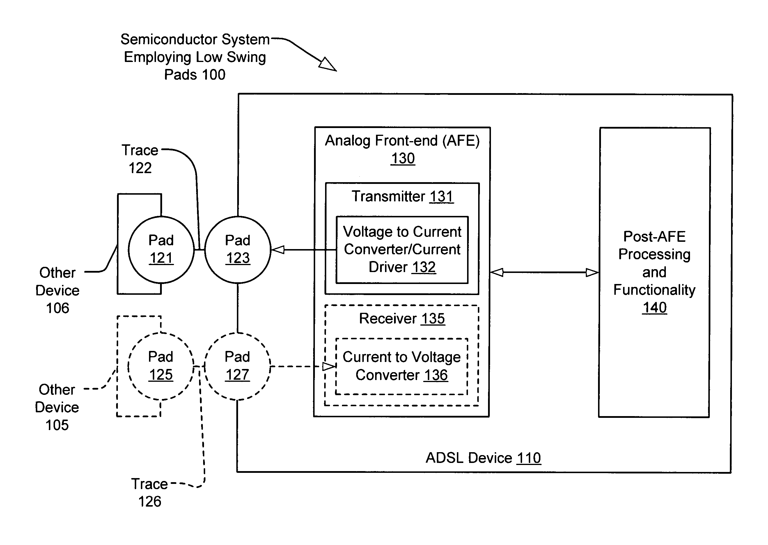
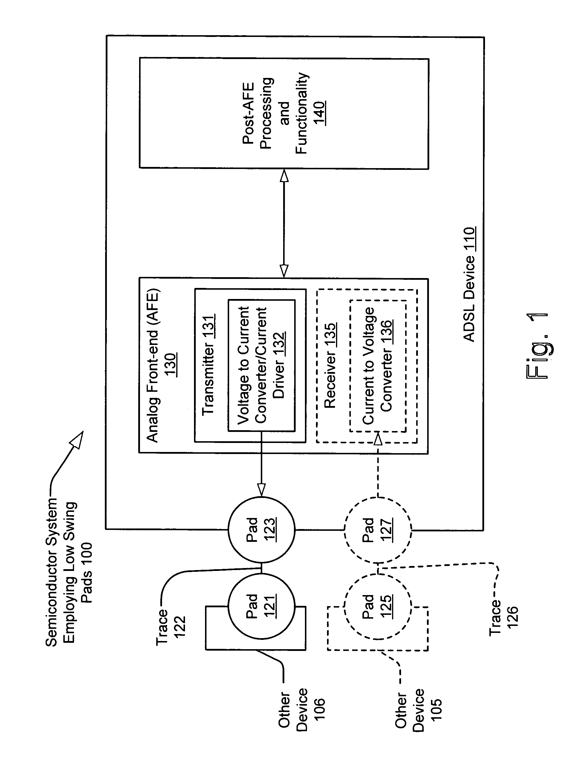
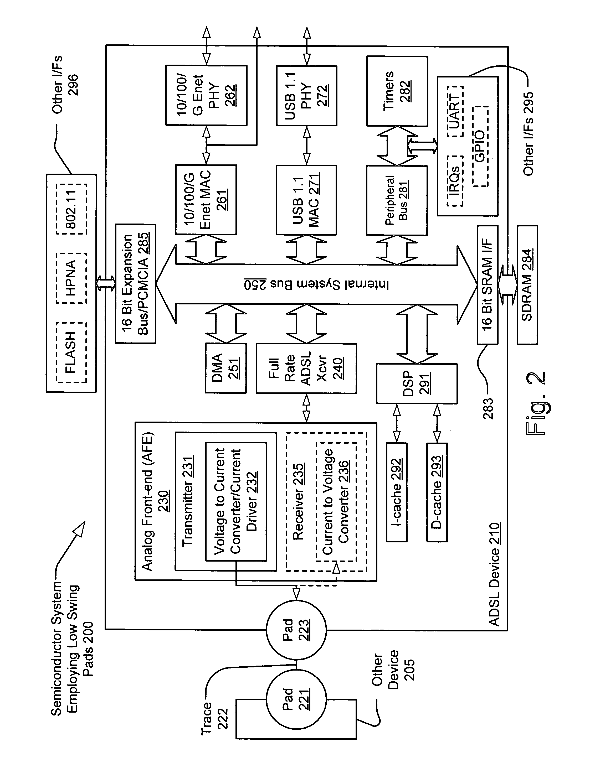
[0028]The present invention provides a much-improved interface between semiconductor devices. Whereas many CMOS devices operate using 0-3.3 V swing voltage signals at many device to device interfaces, the present invention is able to implement a relatively low voltage swing interface by employing current as the data transmitting signal. At a transmitter end, a voltage to current signal conversion is performed. At a receiver end, a current to voltage signal conversion is performed. The present invention may be implemented in a variety of ways. One embodiment involves operating low voltage swing pads within an AFE of an ADSL device. In some embodiments, the ADSL device is a single, integrated semiconductor chip. In addition, in some embodiments, the device or devices may include multiple pads such that each of a transmitter portion and a receiver portion each has a dedicated pad for transmitting and receiving data.

[0029]The low voltage swing pad interface enables a substantial reducti...


PUM


Abstract

Low voltage swing pad driver and receiver. A transmitter portion and a receiver portion are implemented within various devices that communicate using low voltage swing pads communicatively coupled via a trace. The transmitter portion of one device generates a current signal that is pushed / pulled to a low voltage swing pad and is then passed across the trace to another low voltage swing pad. The transmitter portion includes a current driver that outputs the current signal to the low voltage swing pads, and the receiver portion includes a trans-impedance amplifier that transforms the received current signal into a voltage signal. The low voltage swing pad driver and receiver generates a relatively low voltage swing when compared to CMOS full-scale voltage swings thereby significantly reducing the possibility of introducing any noise and / or distortion of data that is communicated via the interface.

Description

CROSS REFERENCE TO RELATED APPLICATIONS[0001]The present U.S. Utility patent application is a continuation of and claims priority pursuant to 35 U.S.C. § 120 to U.S. Utility patent application Ser. No. 10 / 195,966, entitled “LOW VOLTAGE SWING PAD DRIVER AND RECEIVER,” filed Jul. 16, 2002, now U.S. Pat. No. 6,801,577, which is hereby incorporated herein by reference in its entirety and made part of the present U.S. Utility Patent Application for all purposes.[0002]The U.S. Utility patent application Ser. No. 10 / 195,966 claims priority pursuant to 35 U.S.C. § 119(e) to U.S. Provisional Patent Application Ser. No. 60 / 351,708, entitled “LOW VOLTAGE SWING PAD DRIVER AND RECEIVER,” filed Jan. 24, 2002, now abandoned, which is hereby incorporated herein by reference in its entirety and is made part of the present U.S. Utility Patent Application for all purposes.TECHNICAL FIELD OF THE INVENTION[0003]The invention relates generally to semiconductor devices; and, more particularly, it relates ...

Claims


Application Information

Patent Timeline
Patent Type & Authority Patents(United States)
IPC IPC(8): H04L27/00
CPCH04L27/0002
Inventor RANGANATHAN, SUMANTKWAN, TOM W.
Owner AVAGO TECH INT SALES PTE LTD
Learn More