
Systems and methods for using a single reference cell in a dual bit flash memory

a reference cell and flash memory technology, applied in the field of flash based devices, can solve the problems of reduced read margin, affecting the accuracy of data storage in core cells, etc., and achieve the effect of accurate data storage determination

Active Publication Date: 2007-10-30
MACRONIX INT CO LTD
View PDF4 Cites 20 Cited by
  • Summary
  • Abstract
  • Description
  • Claims
  • Application Information

AI Technical Summary

Benefits of technology

This approach maintains accurate data determination and sufficient read margin throughout the life of the device, reducing size and increasing density by using a single reference array and minimizing the impact of charge gain and loss effects.

Problems solved by technology

This approach to reading a core cell has its own problem near the “end of life” for the cell.
The diverging Vt levels between the core cells and the reference cells in conventional dual bit flash memory devices can result in read errors, or what is often referred to as a reduced read margin.
A problem with this approach is that each cell's threshold voltage Vt can vary due to processing differences and differing effects for operations such as erase, program, read, etc.
A draw back to this approach is that it takes a lot of time and that the average Vt is still hard to controlled.

Method used


Image

  • Systems and methods for using a single reference cell in a dual bit flash memory
  • Systems and methods for using a single reference cell in a dual bit flash memory
  • Systems and methods for using a single reference cell in a dual bit flash memory

Examples


Embodiment Construction

.”

BRIEF DESCRIPTION OF THE DRAWINGS

[0012]Features, aspects, and embodiments of the inventions are described in conjunction with the attached drawings, in which:

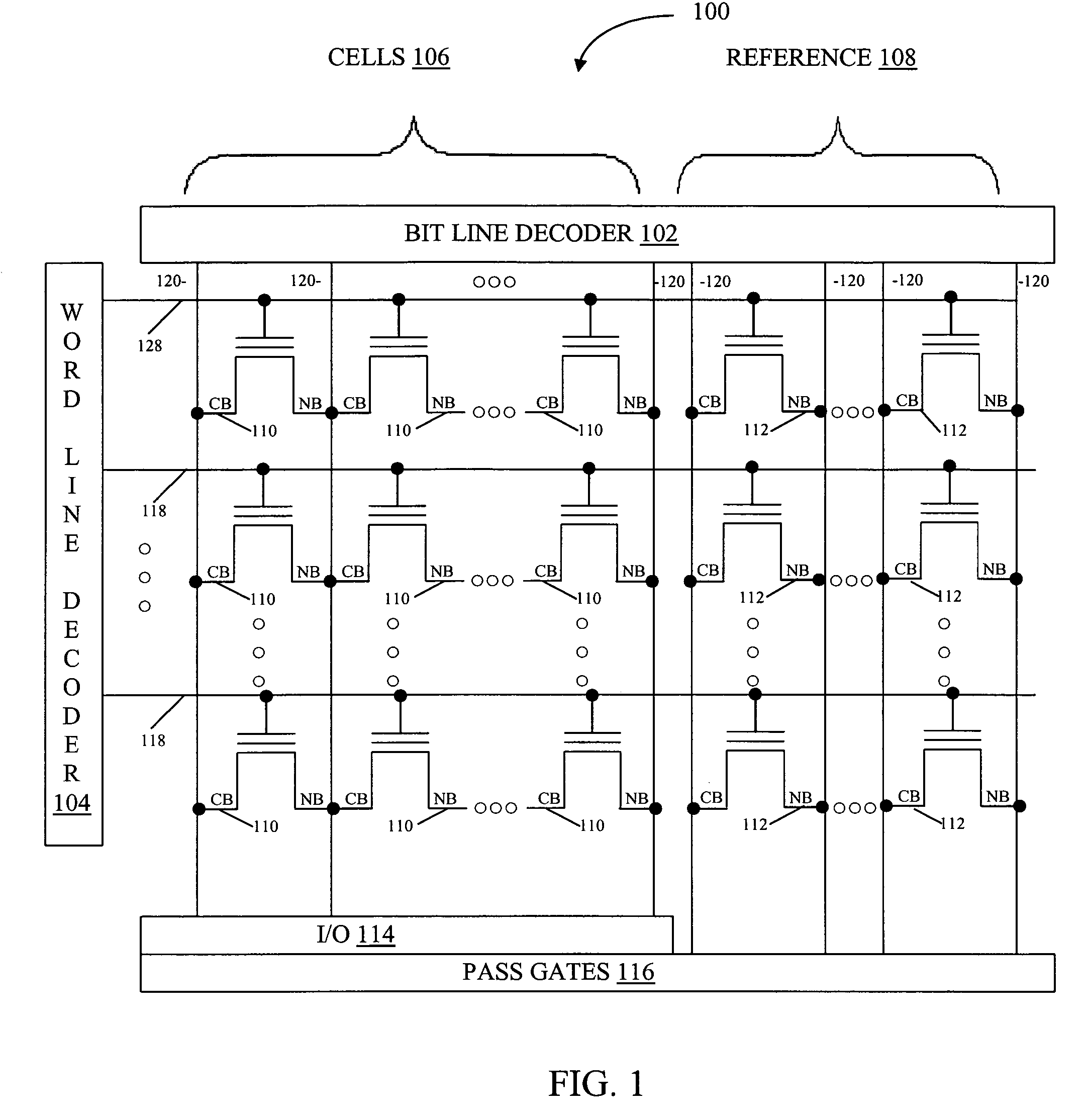
[0013]FIG. 1 is diagram illustrating an example dual bit flash memory architecture in accordance with one embodiment;

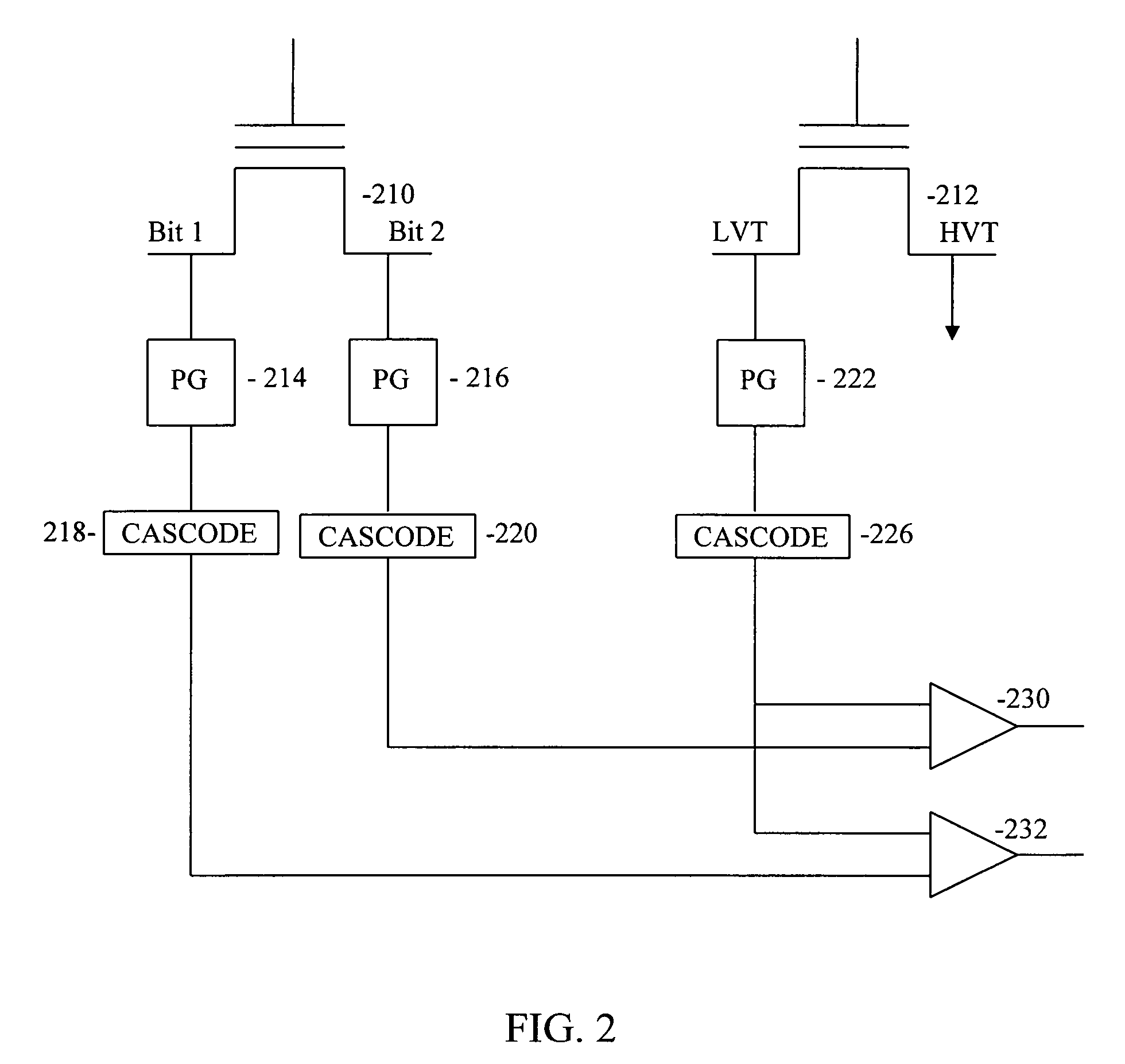
[0014]FIG. 2 is a diagram illustrating the operation of the device of FIG. 1 with respect to a single core cell and a single reference cell;

[0015]FIG. 3 is a flow chart illustrating an example method of operation for the device of FIG. 1 in accordance with one embodiment; and

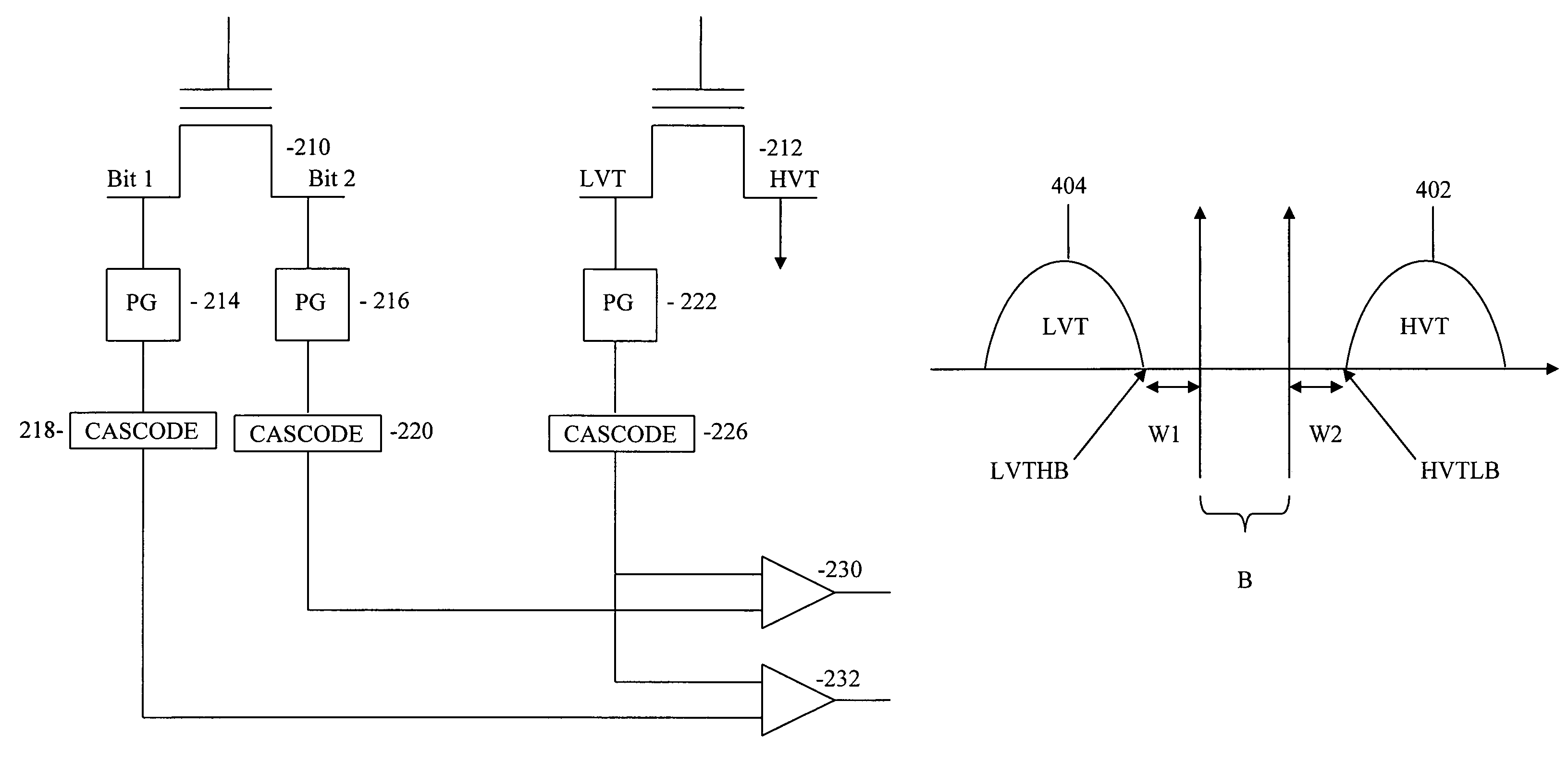
[0016]FIG. 4 is a diagram illustrating an example threshold voltage distribution for reference cells in the device of FIG. 1.

DETAILED DESCRIPTION OF THE PREFERRED EMBODIMENTS

[0017]FIG. 1 is a diagram illustrating an example dual bit flash device 100 configured in accordance with one embodiment of the systems and methods described herein. Device 100 comprises dual bit flash cells 110 and 112. Cells 110 comprise an array of core cells 106, wh...


PUM


Abstract

A dual bit flash device comprising a core cell array, each cell of the core cell array is configured to store two bits of data, and a single reference array, each cell of the single reference array comprising a first bit programmed to a low threshold voltage and a second bit programmed to a high threshold voltage.

Description

BACKGROUND[0001]1. Field of the Invention[0002]The invention relates generally to flash based devices and more particularly to reference circuits and methods for programming reference circuits in dual bit flash memory devices.[0003]2. Background of the Invention[0004]In dual bit flash memory cells, a single cell holds two bits of information. One of the two bits is often referred to as the Normal Bit (NB), while the other is often referred to as the Complimentary Bit (CB). Dual bit flash memory cells use what is known as virtual ground architectures in which the source for one of the two bits serves as the drain for the other. In other words, the cell essentially comprises a gate and two terminals. For one of the two bits, one of the two terminals is the source and the other is the drain. But for the other bit, the function of the two terminals is alternated, such that the terminal that was the source for the first bit is now the drain for the second bit, and vise versa.[0005]In a c...

Claims


Application Information

Patent Timeline
Patent Type & Authority Patents(United States)
IPC IPC(8): G11C11/34
CPCG11C16/28G11C16/0475
Inventor KUO, NAI-PINGCHEN, HAN-SUNGCHEN, KEN-HUIHUNG, CHUN-HSIUNG
Owner MACRONIX INT CO LTD
Learn More