
Stress-free lead frame

a lead frame and stress-free technology, applied in the field of stress-free lead frame, can solve the problems of mlp reject, lead frame subject to tremendous structural stress, package reliability failure, etc., and achieve the effect of removing lead delamination

Inactive Publication Date: 2007-10-30
CARSEM M
View PDF48 Cites 5 Cited by
  • Summary
  • Abstract
  • Description
  • Claims
  • Application Information

AI Technical Summary

Benefits of technology

The stress-relief and interlocking means effectively eliminate delamination, ensuring reliable packaging by accommodating thermal expansion and contraction, thereby reducing packaging failures and rejects.

Problems solved by technology

This is undesirable as it will cause damage and thus render the MLP a reject.
The moulding step also subjects the lead frame to tremendous structural stresses caused by the difference in expansion and compression of the moulded metallic foil that the lead frame and the unmoulded metallic foil that is its outer periphery.
This causes bending, waving and twisting of the leads, resulting in delamination of the leads or separation of the metallic lead frame and the epoxy which will results in reliability failure of the package.

Method used


Image

  • Stress-free lead frame
  • Stress-free lead frame
  • Stress-free lead frame

Examples


Embodiment Construction

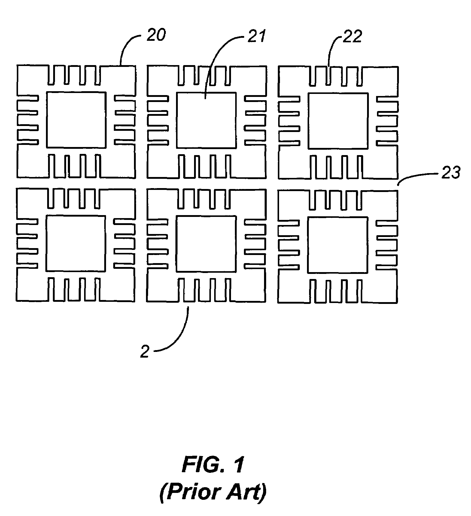
[0019]Referring now to FIG. 1 showing a lead frame of the prior art having a multiple integrated circuit units. A lead frame (2) of the prior art consists of a plurality of integrated circuits (20), each having a die pad (21) and a plurality of leads (22) projecting outwardly from the die pad (21). The integrated circuits (20) are connected together by connecting bars (23). At the outer periphery of the lead frame (2), there is an inactive portion of the lead frame (2) called a peripheral pad (not shown). When the lead frame (2) is moulded to form the MLP, about half of the peripheral pad is left unmoulded causing different expansions and thus delamination to the plurality of leads (22) adjacent to the peripheral pad.

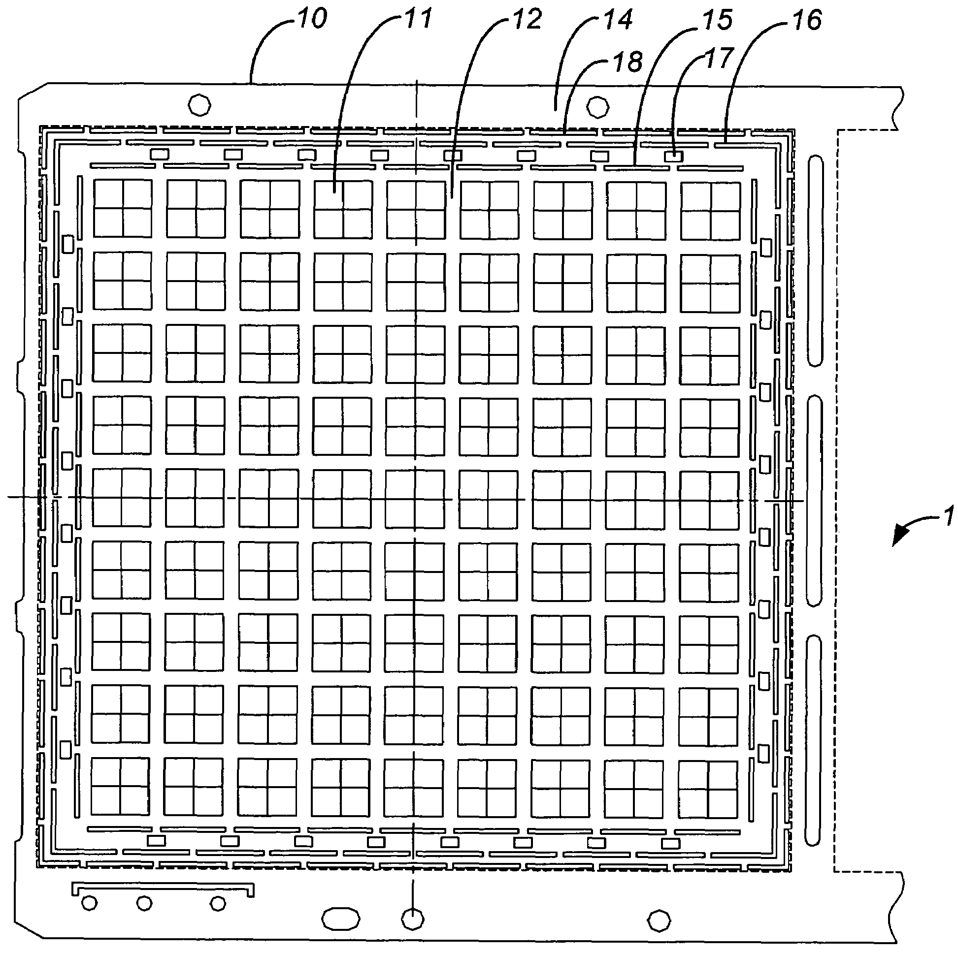
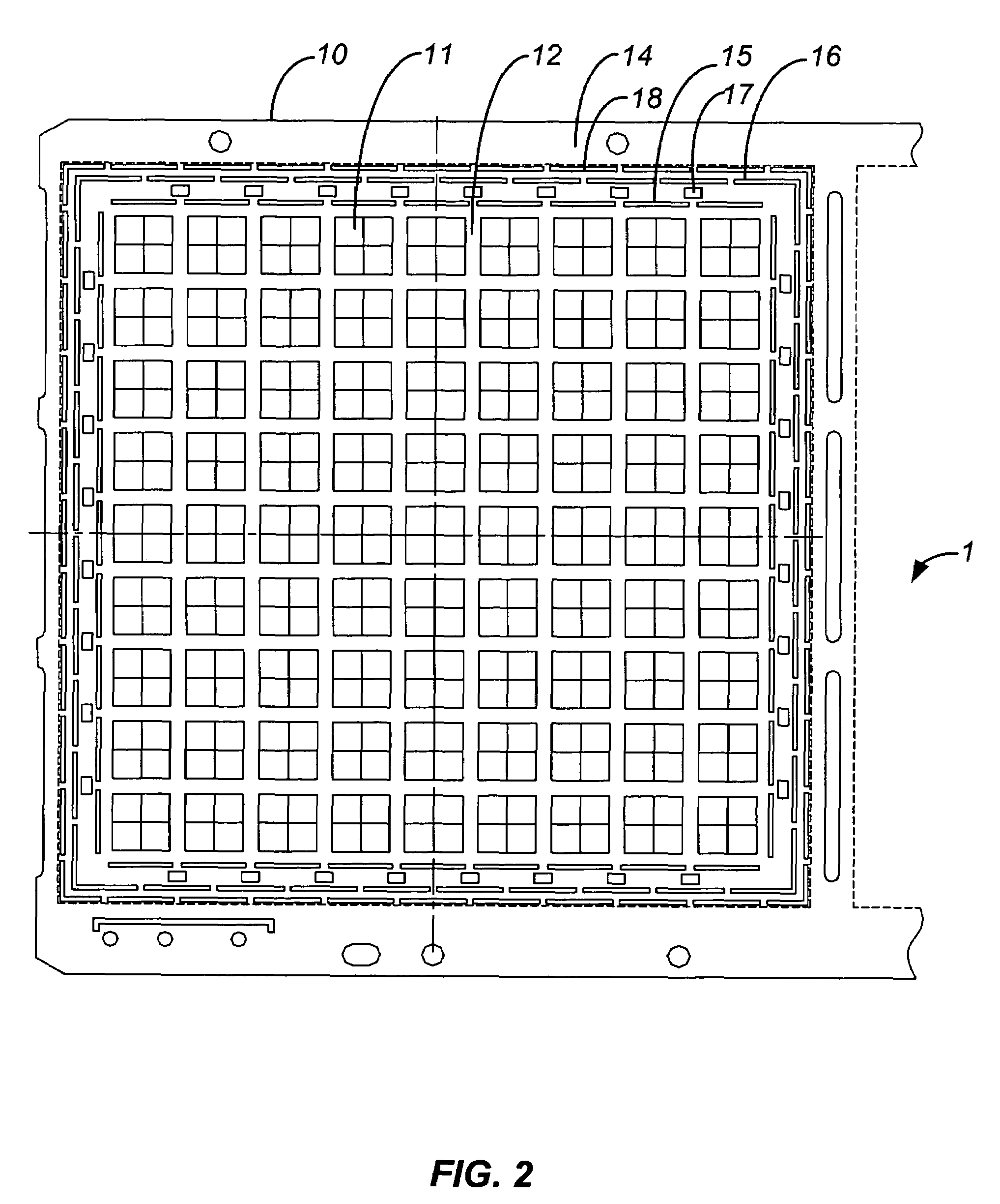
[0020]Referring to FIG. 2 showing a stress-free lead frame having a stress-relief means according to one embodiment of the present invention. The stress-free lead frame (1) comprises a lead frame (10) having a plurality of integrated circuit areas or integrated circuits...


PUM


Abstract

The present invention relates to a stress-free lead frame (1) for a semiconductor. The stress-free lead frame (1) is provided with a stress-relief means (15) and an interlocking means (16) at the outer periphery. The stress-relief means (15) is capable of accommodating expansion and compression while the interlocking means (16) take care of shock and vibration during handling to thereby eliminate delamination of the lead frame (10).

Description

CROSS-REFERENCES TO RELATED APPLICATIONS[0001]This application is a continuation of U.S. application Ser. No. 09 / 909,934, filed Jul. 20, 2001 now U.S. Pat. No. 6,867,483, entitled “Stress-Free Lead Frame,” having Lee Kock Huat et al. listed as coinventors. The disclosure of Ser. No. 09 / 909,934 is herein incorporated herein by reference in its entirety.FIELD OF THE INVENTION[0002]The present invention relates generally to a lead frame, especially to a stress-free lead frame for semiconductor provided with a stress-relief means and an interlocking means for eliminating delamination of leads during packaging.BACKGROUND OF THE INVENTION[0003]The process of manufacturing semiconductor devices involves several steps whereby an integrated circuit chip is bonded to a foil-type lead frame and encapsulated in epoxy or other moulded resin. The lead frame comprises of a plurality of leads etched or stamped out of a thin metallic foil sheet, and the inner ends of the leads are usually bonded to ...

Claims


Application Information

Patent Timeline
Patent Type & Authority Patents(United States)
IPC IPC(8): H01L23/495
CPCH01L21/561H01L23/49541H01L23/49565H01L24/97H01L2924/14H01L2224/97H01L2224/81
Inventor HUAT, LEE KOCKMENG, CHAN BOONTUCK, CHEONG MUNSIN, LEE HUANKEUNG, PHUAH KIANETURAJULU, ARAVENTHANKENG, LIOW ENGKONG, THUM MINHING, CHEN CHOON
Owner CARSEM M
Learn More