Front-illuminated-type photodiode array
a photodiode array and front-illuminated technology, applied in the direction of electrical equipment, semiconductor devices, radio control devices, etc., can solve the problems of optical crosstalk, deterioration of the pn junction, and other problems, and achieve the effect of preventing optical crosstalk
- Summary
- Abstract
- Description
- Claims
- Application Information
AI Technical Summary
Benefits of technology
Problems solved by technology
Method used
Image
Examples
example 1
One-dimensionally Arranged Photodiode Array (Above Type: M×1)
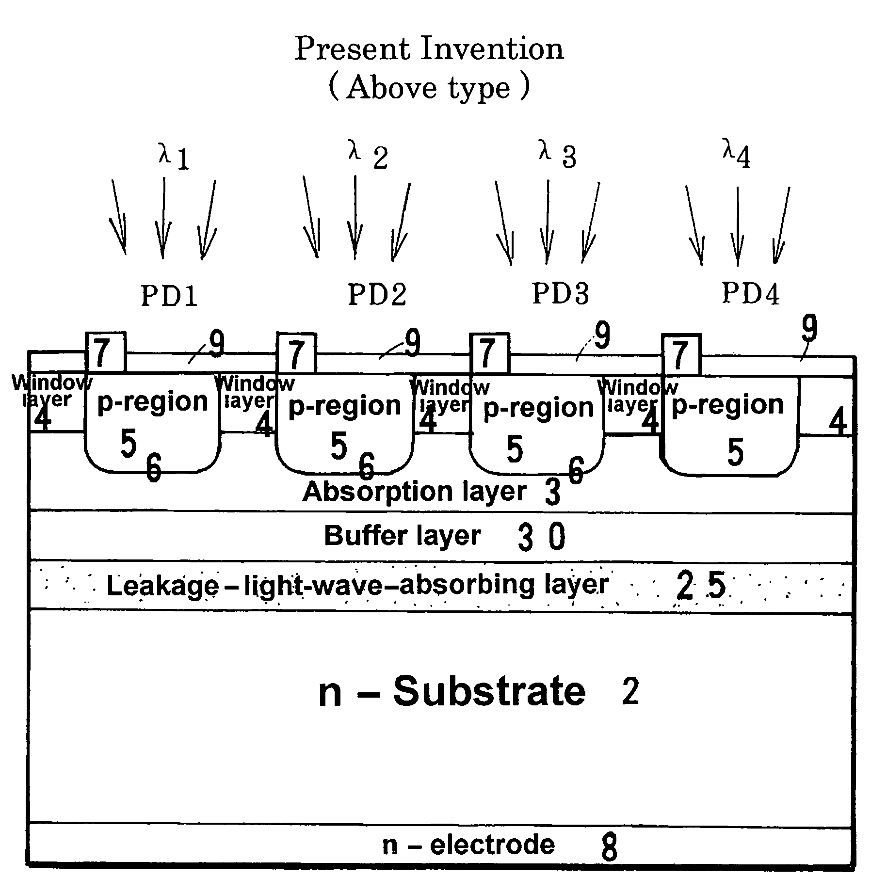
[0062]An embodiment of an above-type photodiode array of the present invention that has a leakage-lightwave-absorbing layer provided above the substrate (see FIG. 5) is explained below by referring to FIG. 9. Although FIG. 9 shows an array having four unit photodiodes, the number of unit photodiodes may be increased. When an array has a specific number of photodiode units such that the number is expressed as a power of two such as eight, 16, 32, and so on, the array is suitable for a receiving section of optical communication. It is recommended that the pitch of the arrangement be either the same as the diameter of the cladding of the optical fiber (125 μm) or an integral multiple of the diameter. For an optical sensor in which a plurality of photodiode units are arranged one-dimensionally, both the number of photodiode units M and the pitch P can be determined freely in accordance with the purpose.
[0063]In Example 1, the ...
example 2
Two-dimensionally Arranged Photodiode Array (Above Type: M×N)
[0076]The present invention can also be applied to a front-illuminated-type two-dimensionally arranged photodiode array. FIG. 10 shows a partial plan view of it, and FIG. 11 a partial cross-sectional view of it. This array is formed by arranging photodiode units, “M×N” in number, on one chip. When viewed from above, p-regions 5 and p-electrodes 7 are arranged in rows and columns. Actually, the top surface is covered with an antireflective coating 9 and the p-electrodes 7 complementarily. A number of electrode pads 40 connected to the p-electrodes are provided at one, two, three, or four sides of the chip. The electrode pads 40 are connected through wires 42 to the p-electrodes 7 of the individual photodiode units. An n-electrode 8 is common and placed at the rear side of the chip. Consequently, it is bonded to a stem of a package. The electrode pads 40 are connected to pins of the package by wire bonding.
[0077]As shown in ...
PUM
 Abstract
Description
Claims
Application Information
 - R&D
- Intellectual Property
- Life Sciences
- Materials
- Tech Scout
- Unparalleled Data Quality
- Higher Quality Content
- 60% Fewer Hallucinations
Browse by: Latest US Patents, China's latest patents, Technical Efficacy Thesaurus, Application Domain, Technology Topic, Popular Technical Reports.
© 2025 PatSnap. All rights reserved.Legal|Privacy policy|Modern Slavery Act Transparency Statement|Sitemap|About US| Contact US: help@patsnap.com


