Power supply circuit including stably operating voltage regulators
- Summary
- Abstract
- Description
- Claims
- Application Information
AI Technical Summary
Benefits of technology
Problems solved by technology
Method used
Image
Examples
first embodiment
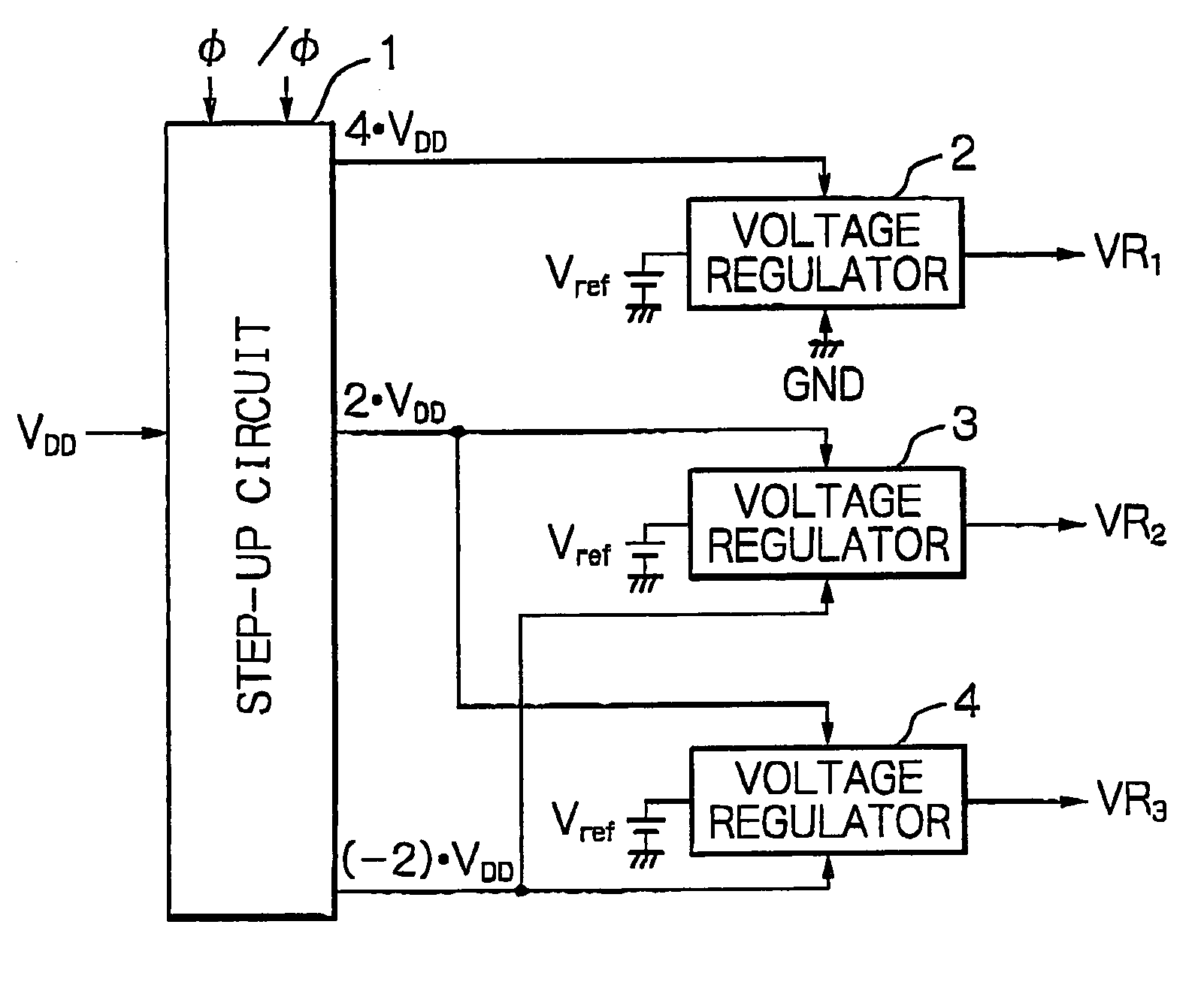
[0045]In FIG. 7, which illustrates the power supply circuit according to the present invention, the voltage regulator 3 of FIG. 2 is powered by the voltage 2·VDD and the voltage (−2)·VDD, and the voltage regulator 4 of FIG. 2 is powered by the voltage 2·VDD and the voltage (−2)·VDD. That is, all the voltage regulators 2, 3 and 4 are powered by the large voltage difference 4·VDD.
[0046]Thus, the absolute threshold voltages of the MOS transistors of all the voltage regulators 2, 3 and 4 can be increased-to operate the MOS transistors, so that the breakdown voltage can be enhanced. Also, in this case, since the MOS transistors can be replaced by TFTs having large absolute threshold voltages, the manufacturing cost of the LCD apparatus of FIG. 1 would be decreased. Note that the step-up circuit 1 of FIG. 1 can also be formed by TFTs, which further would decrease the manufacturing cost of the LCD apparatus of FIG. 1.
second embodiment
[0047]In FIG. 8, which illustrates the power supply circuit according to the present invention, the voltage regulator 2 of FIG. 2 is powered by the voltage 4·VDD and the voltage 2·VDD. That is, all the voltage regulators 2, 3 and 4 are powered by the small voltage difference 2·VDD.
[0048]Thus, the absolute threshold voltages of the MOS transistors of all the voltage regulators 2, 3 and 4 can be decreased to operate the MOS transistors. In this case, the breakdown voltage is decreased; however, this would create no problem, since all the voltage regulators 2, 3 and 4 are powered by the small voltage difference.
third embodiment
[0049]In FIG. 9, which illustrates the power supply circuit according to the present invention, the regulated voltages VR1 and VR3 of FIG. 7 are not used; the voltage 4·VDD and the voltage (−2)·VDD are supplied directly to the gate line driver circuit 103 of FIG. 1. That is, in the gate line driver circuit 103, a high current drive ability is not required as explained above, and also, the power consumption is small and the fluctuation of supplied currents is small. Therefore, the gate lines GL can be driven directly by the voltage 4·VDD and (−2)·VDD.
[0050]Thus, in FIG. 9, since the voltage regulators 2 and 4 of FIG. 7 are unnecessary, the manufacturing cost of the LCD apparatus of FIG. 1 can be decreased.
[0051]As explained hereinabove, according to the present invention, all the voltage regulators can be stably operated and, also, the reliability can be improved.
PUM
 Abstract
Description
Claims
Application Information
 - R&D
- Intellectual Property
- Life Sciences
- Materials
- Tech Scout
- Unparalleled Data Quality
- Higher Quality Content
- 60% Fewer Hallucinations
Browse by: Latest US Patents, China's latest patents, Technical Efficacy Thesaurus, Application Domain, Technology Topic, Popular Technical Reports.
© 2025 PatSnap. All rights reserved.Legal|Privacy policy|Modern Slavery Act Transparency Statement|Sitemap|About US| Contact US: help@patsnap.com


